PCB Assembly
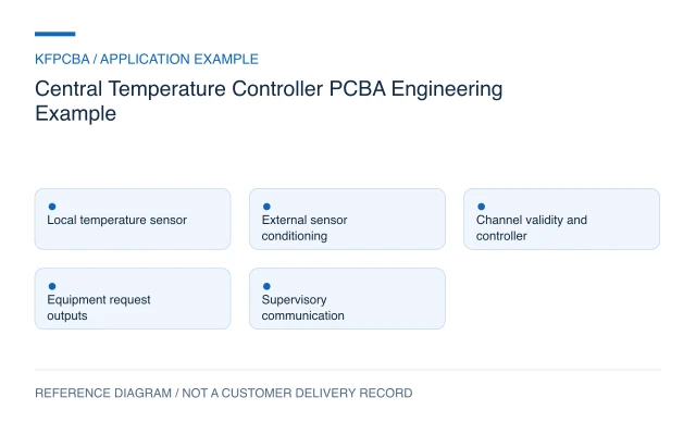
Central Temperature Controller PCBA Engineering Example
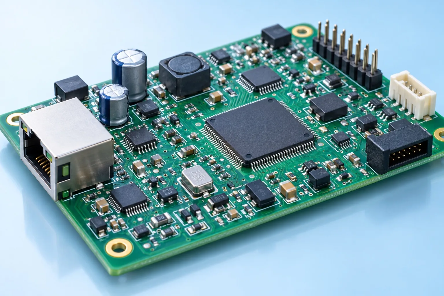
Illustrative central temperature-controller PCBA example covering local sensing, external sensor interfaces, output mapping and communication timing.
View Example

Identify the documents your project requires, then verify the holder, site, scope and validity. These topics do not establish certification for a particular order.
For automotive projects, request the applicable certificate and verify its holder, site, scope and validity.
If required for supplier qualification, request the current quality-management certificate for the intended operator and site.
Review environmental-management evidence for the intended site against your supplier requirements.
For medical-electronics projects, verify the applicable quality-system evidence and certified activities.
Check any required UL file against the actual material, product category, site and order scope.
If relevant to the shipment, request evidence of the operator's customs authorization and current status.

KFPCBA was established in December 2020 in Shenzhen. We discuss PCB fabrication, PCB assembly, component sourcing and electronics development against project-specific files.
Materials, sourcing, inspection, testing, schedule, and production-site allocation are confirmed against the released project data before an order is accepted.
Explore illustrative PCB and assembly applications, design choices, verification plans and RFQ inputs. These examples are not customer delivery records.
Illustrative central temperature-controller PCBA example covering local sensing, external sensor interfaces, output mapping and communication timing.
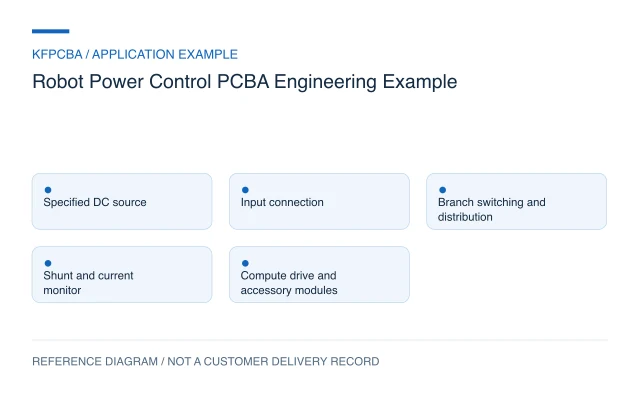
View ExampleIllustrative robot power-control PCBA example covering branch connections, current monitoring, startup sequencing and module handoff.
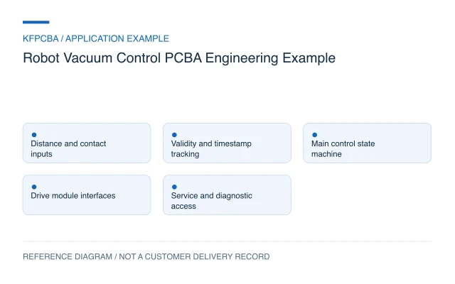
View ExampleIllustrative robot-vacuum control PCBA example covering sensor status, drive commands, optical integration and revision-controlled tests.
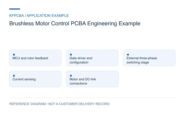
View ExampleIllustrative brushless-motor control PCBA example covering the gate driver, external power stage, current sensing and mixed-technology assembly.
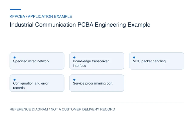
View ExampleIllustrative industrial communication-control PCBA example covering the physical link, packet timing, board-edge connectors and diagnostic records.
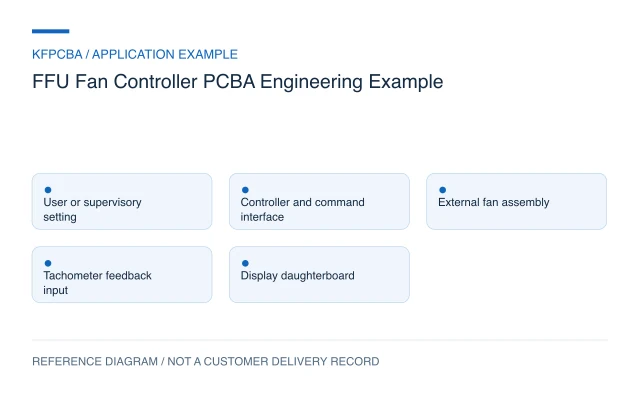
View ExampleIllustrative filter fan unit controller PCBA example covering fan command and feedback interfaces, daughterboard fit and module-test boundaries.
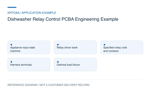
View ExampleIllustrative dishwasher control PCBA example covering relay selection inputs, terminal mapping, control-supply demand and verification planning.
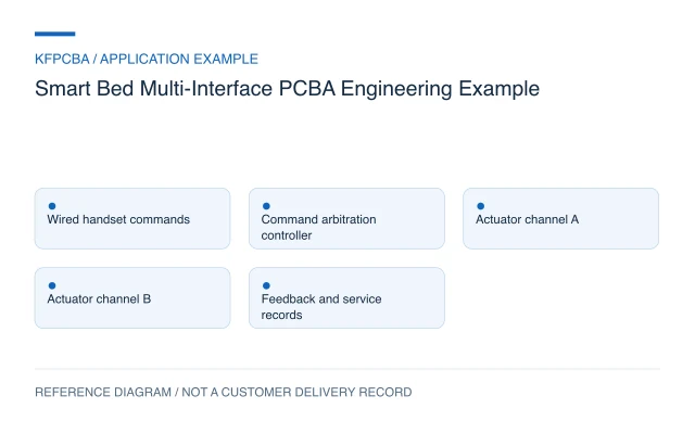
View ExampleIllustrative smart-bed control PCBA example covering wired controls, actuator interfaces, connector identification and position-feedback records.
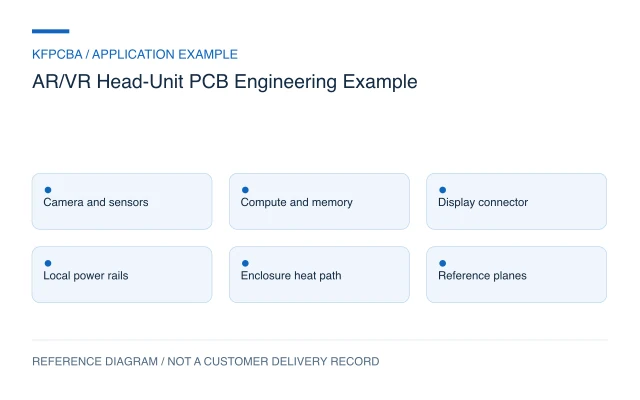
View ExamplePlan an AR/VR compute and display board around actual interfaces, mechanical space, heat sources and verification evidence before choosing layer count.
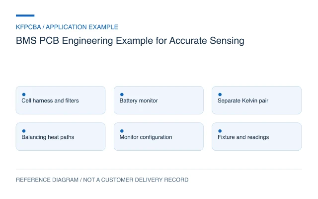
View ExampleReview a BMS PCB by separating sensitive measurement paths, balancing heat and power-current routing, with a traceable error budget and test plan.
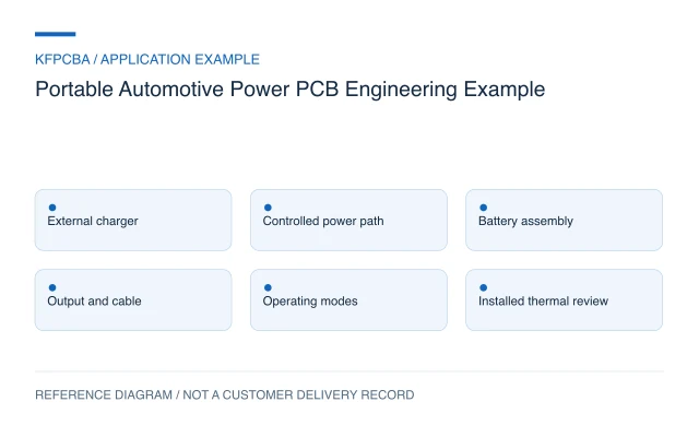
View ExampleDefine the energy source, charging and output modes before deciding how a portable automotive power PCB should route current and manage heat.
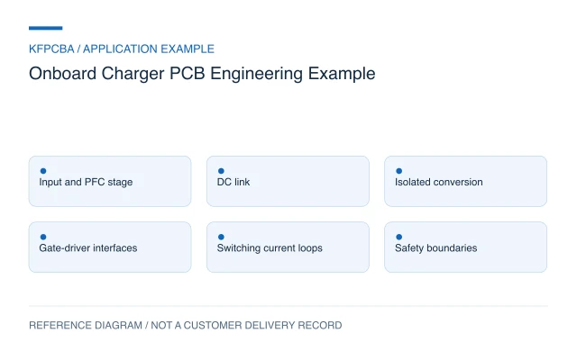
View ExampleReview an onboard-charger PCB by separating power-current routing, fast switching loops, isolation boundaries and control measurements before choosing copper weight.
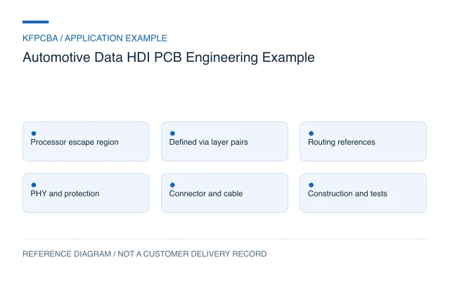
View ExampleChoose an HDI structure for an automotive data board by proving the package escape and channel routing, then defining every via span and verification record.
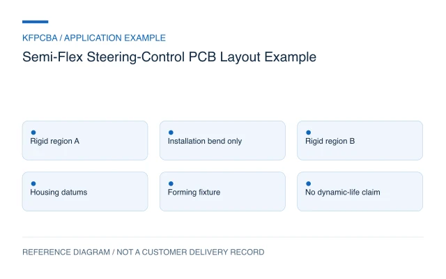
View ExampleAssess a semi-flex steering-control board as an installation-geometry problem, with an explicit bend state, mechanical support and controlled assembly sequence.
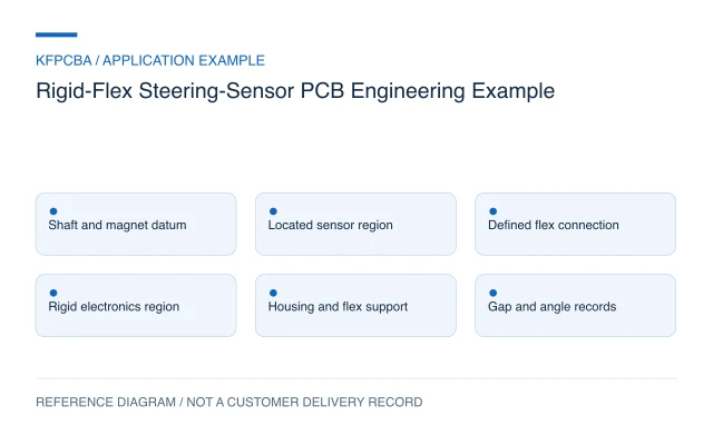
View ExampleUse rigid-flex to connect a located sensor region to a separate electronics region while controlling sensor datums, flex loading and installed geometry.
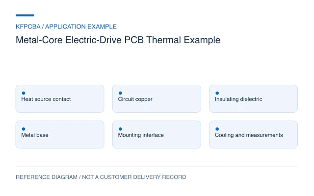
View ExampleAssess an electric-drive metal-core PCB through the complete heat path, from the component contact through the dielectric and mounting interface to the cooling structure.
View Example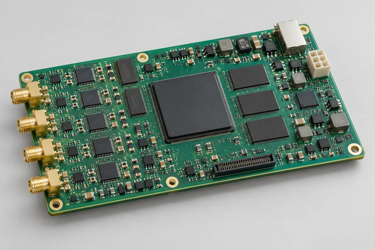 FPGA data acquisition board PCB assemblyEngineering Reference Configuration
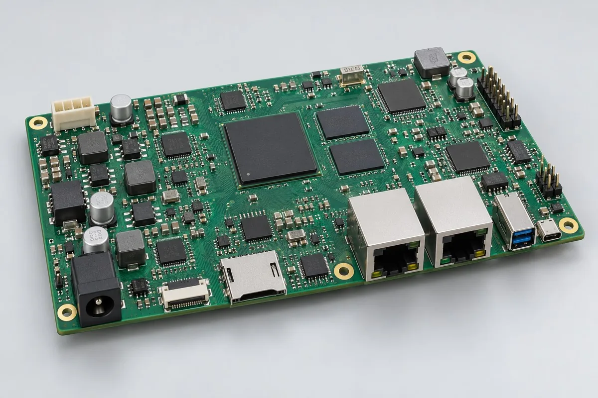 Communication gateway mainboard PCB assemblyEngineering Reference Configuration
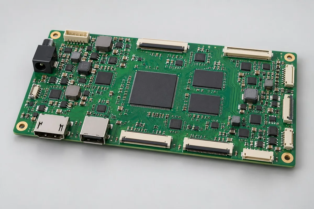 Industrial display motherboard PCB assemblyEngineering Reference Configuration
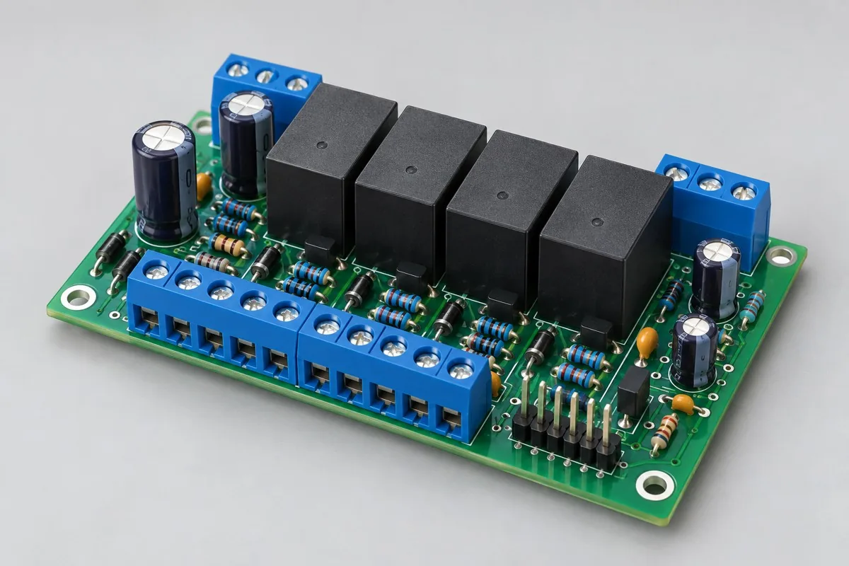 Relay control board through-hole assemblyEngineering Reference Configuration
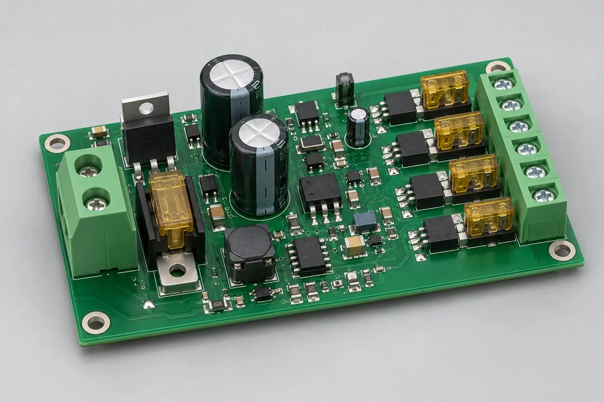 Power interface board through-hole assemblyEngineering Reference Configuration
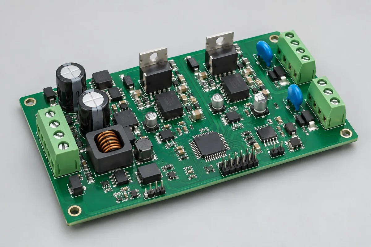 Equipment driver board through-hole assemblyEngineering Reference Configuration
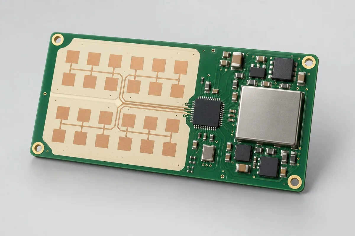 Millimeter-wave radar PCB assemblyEngineering Reference Configuration
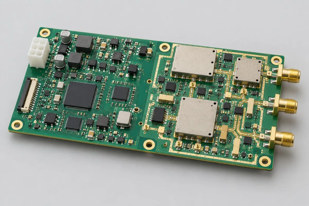 RF transceiver board PCB assemblyEngineering Reference Configuration
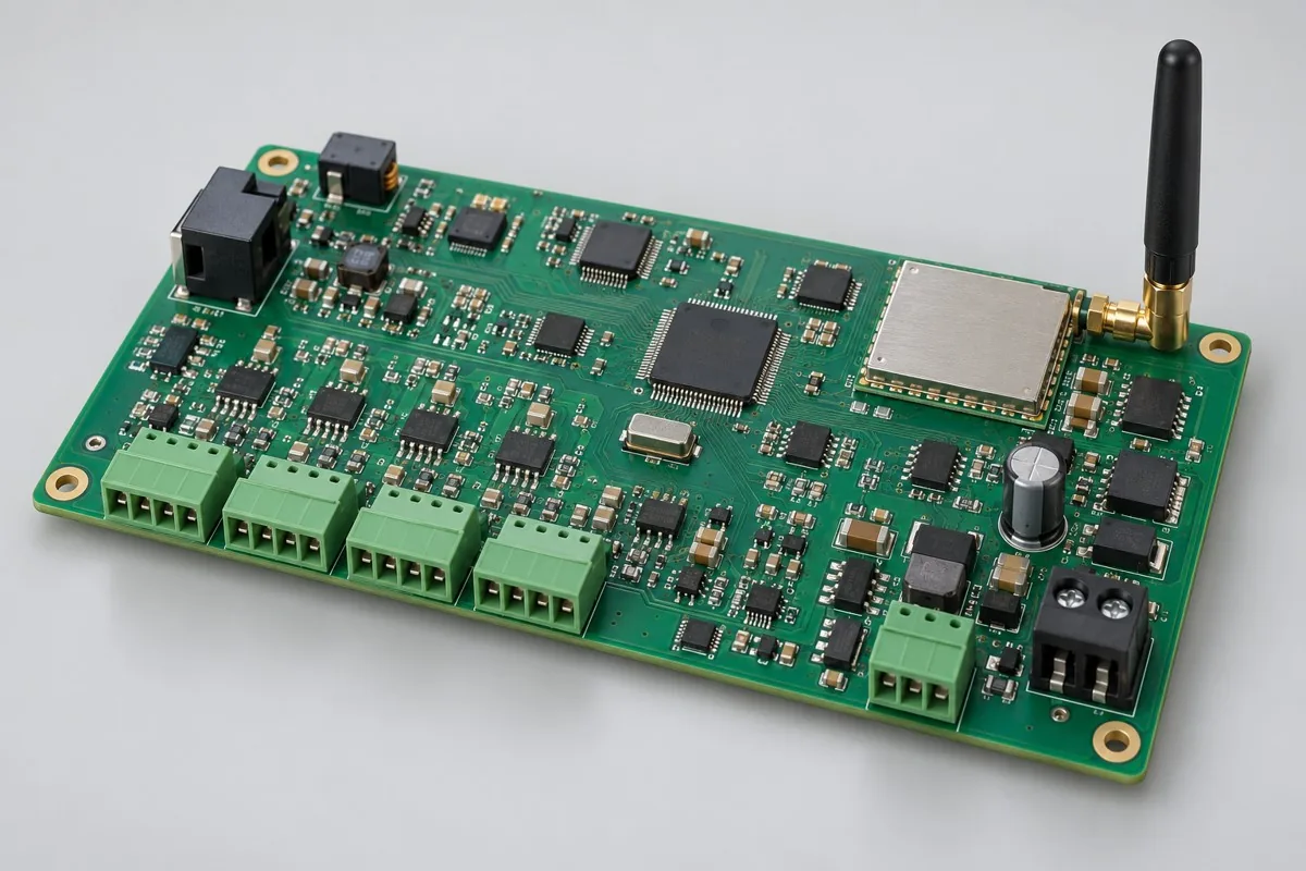 Wireless measurement gateway PCB assemblyEngineering Reference Configuration
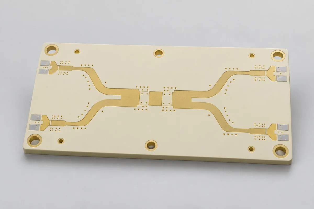 RO4350B high-frequency PCB fabricationEngineering Selection Reference
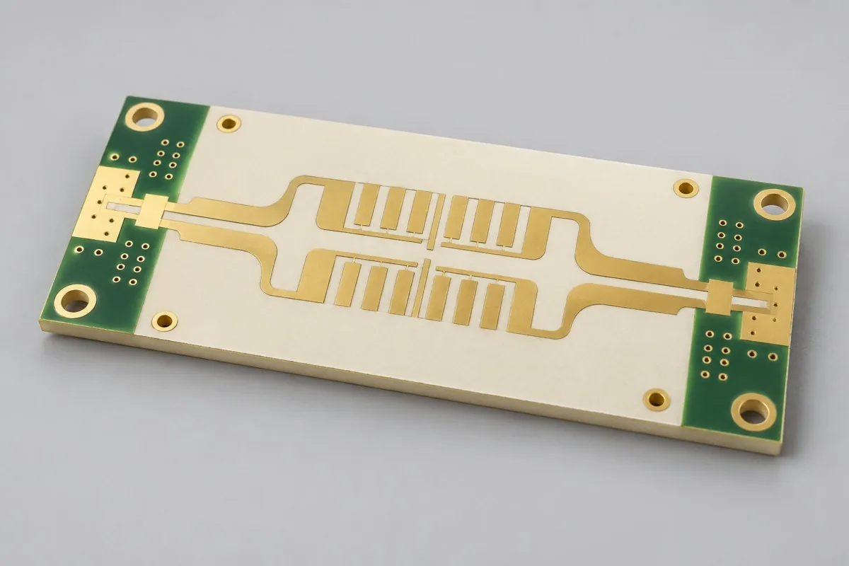 RO4003C High-Frequency Board PrototypingEngineering Selection Reference
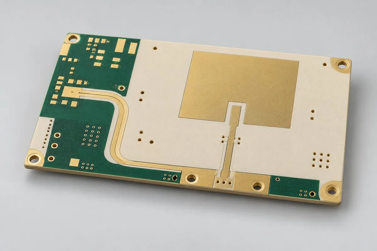 Rogers 5880 antenna PCBEngineering Selection Reference
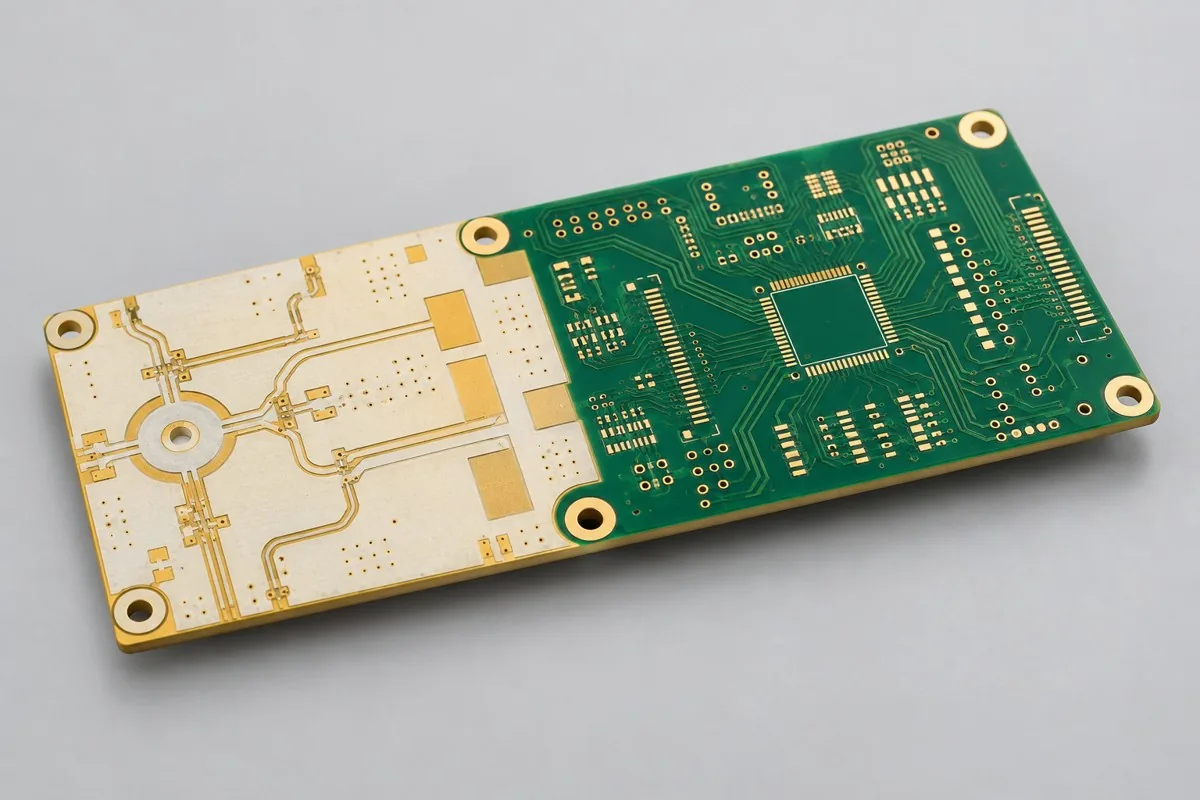 RO4003C hybrid-material PCB fabricationEngineering Selection Reference
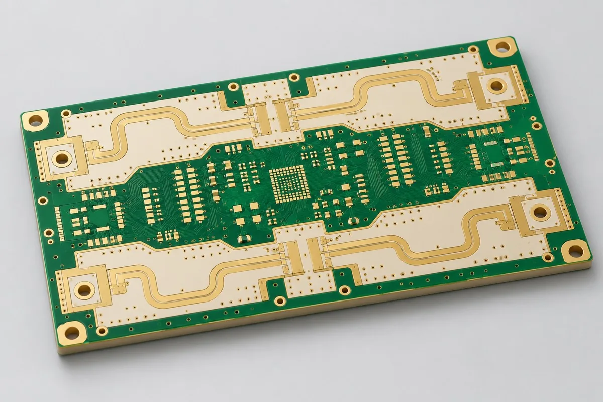 RO4350B eight-layer hybrid PCBEngineering Selection Reference
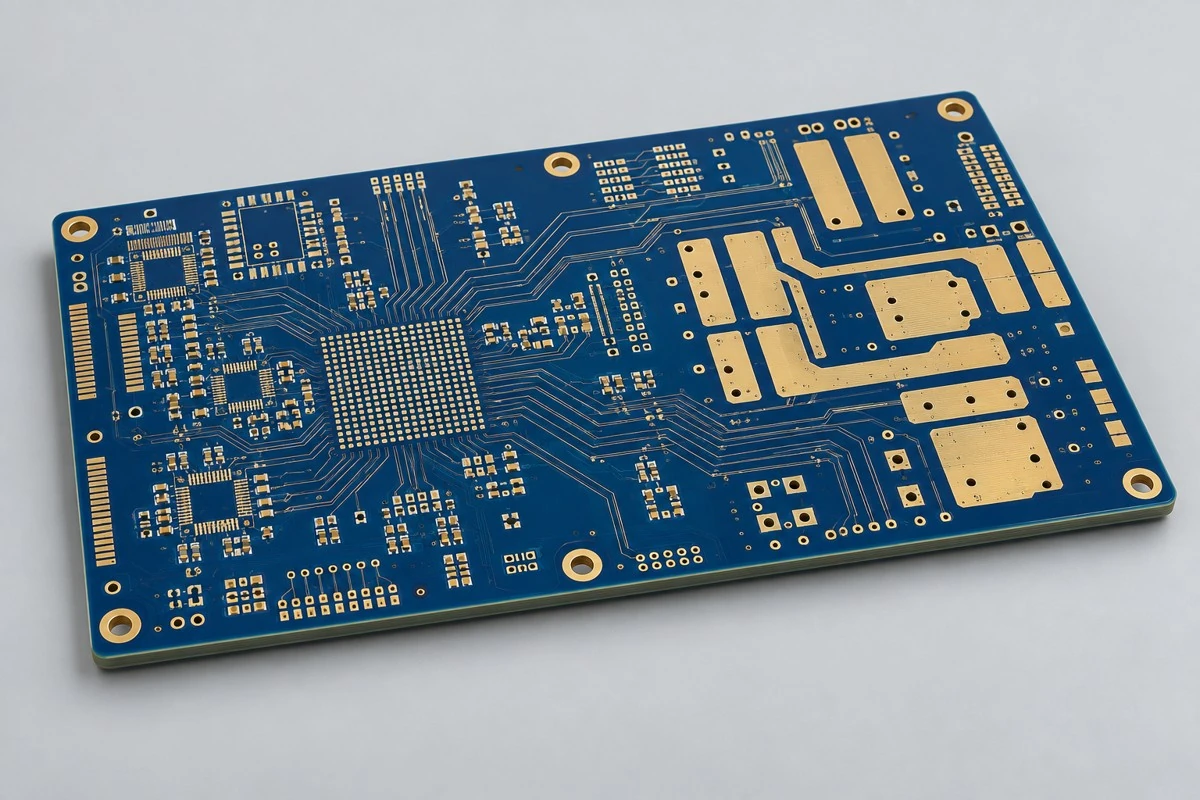 Ten-layer hybrid-laminate PCB fabricationEngineering Selection Reference
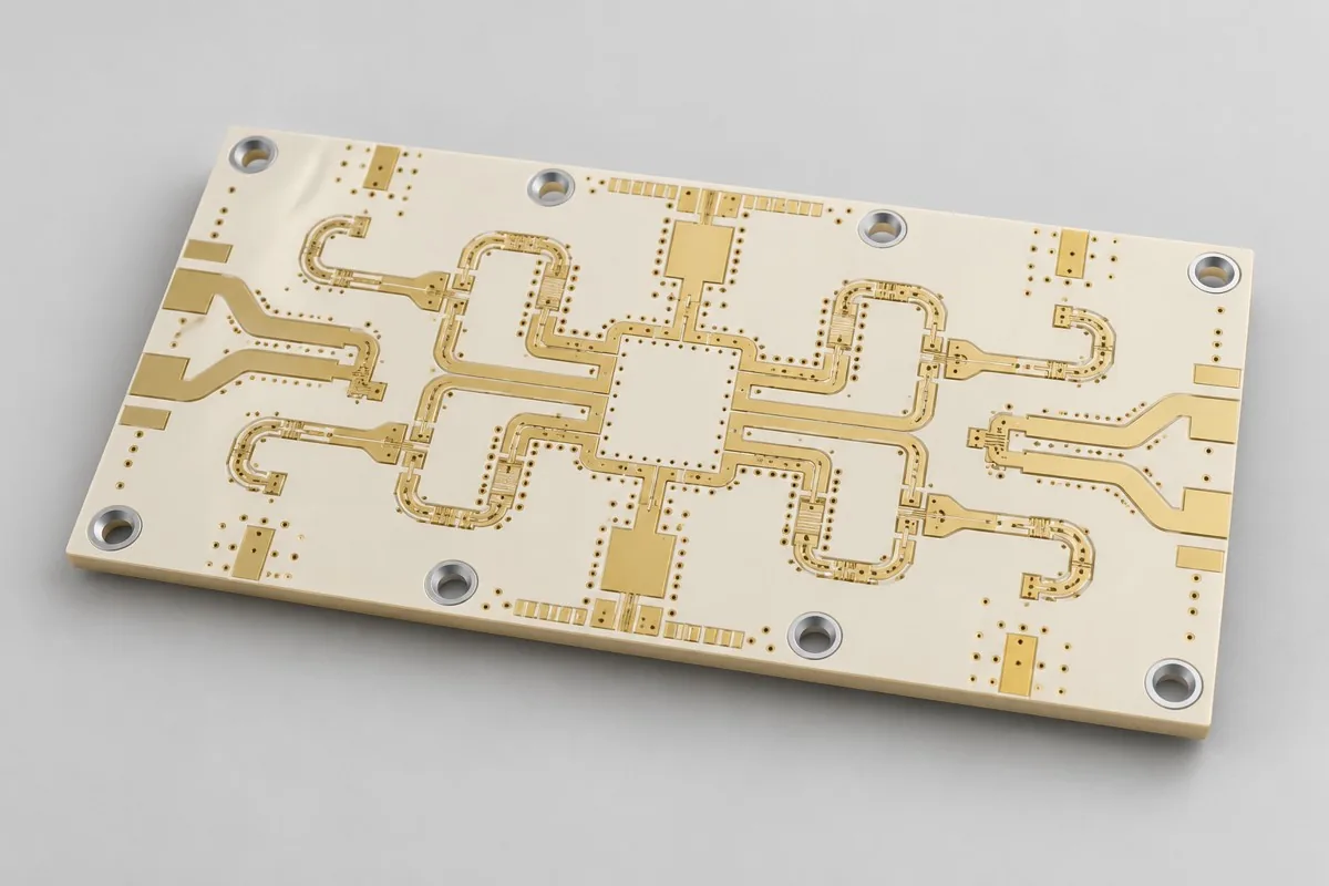 Four-layer RO4350B PCB fabricationEngineering Selection Reference
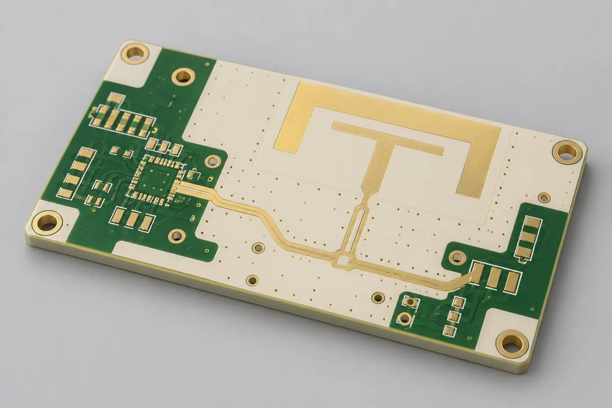 RO3010 antenna PCB fabricationEngineering Selection Reference
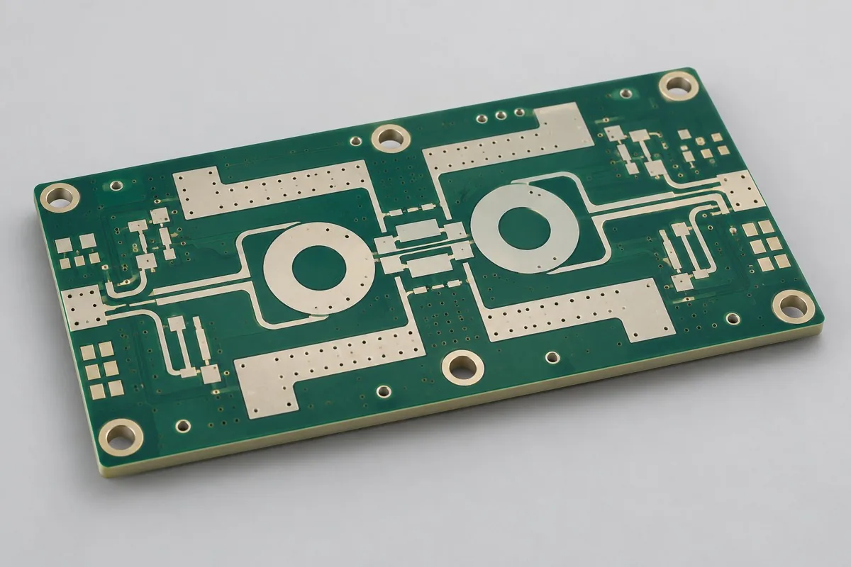 TMM10i PCB fabricationEngineering Selection Reference

Discuss an NDA and define how drawings and BOM data may be used before files are shared.
Coordinate PCB design, DFMA, fabrication, and assembly within one controlled product revision.
Connect incoming, in-process, and outgoing inspection with the acceptance requirements agreed for the project.
Define functions first, then agree the design and verification scope for communications, industrial, or connected products.
Review quantity, supply model, processes, testing, and target date together before issuing a quotation.
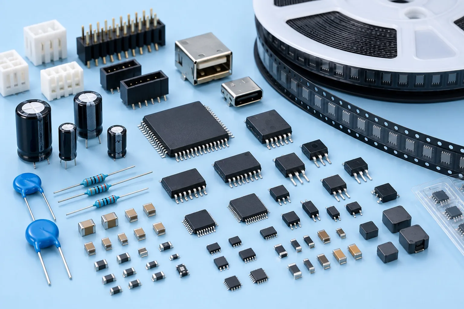
Review the approved BOM, sourcing requirements, and substitution authority before component purchasing.
Match equipment and line planning to component, board, and process requirements during project review.
Coordinate data, material readiness, and production milestones against the confirmed project plan.
Start with the product environment, board structure, and delivery stage to identify the fabrication, assembly, or development support required.

Discuss fabrication, assembly, traceability, and verification requirements for acquisition, control, and interface boards.
Explore Industry Requirements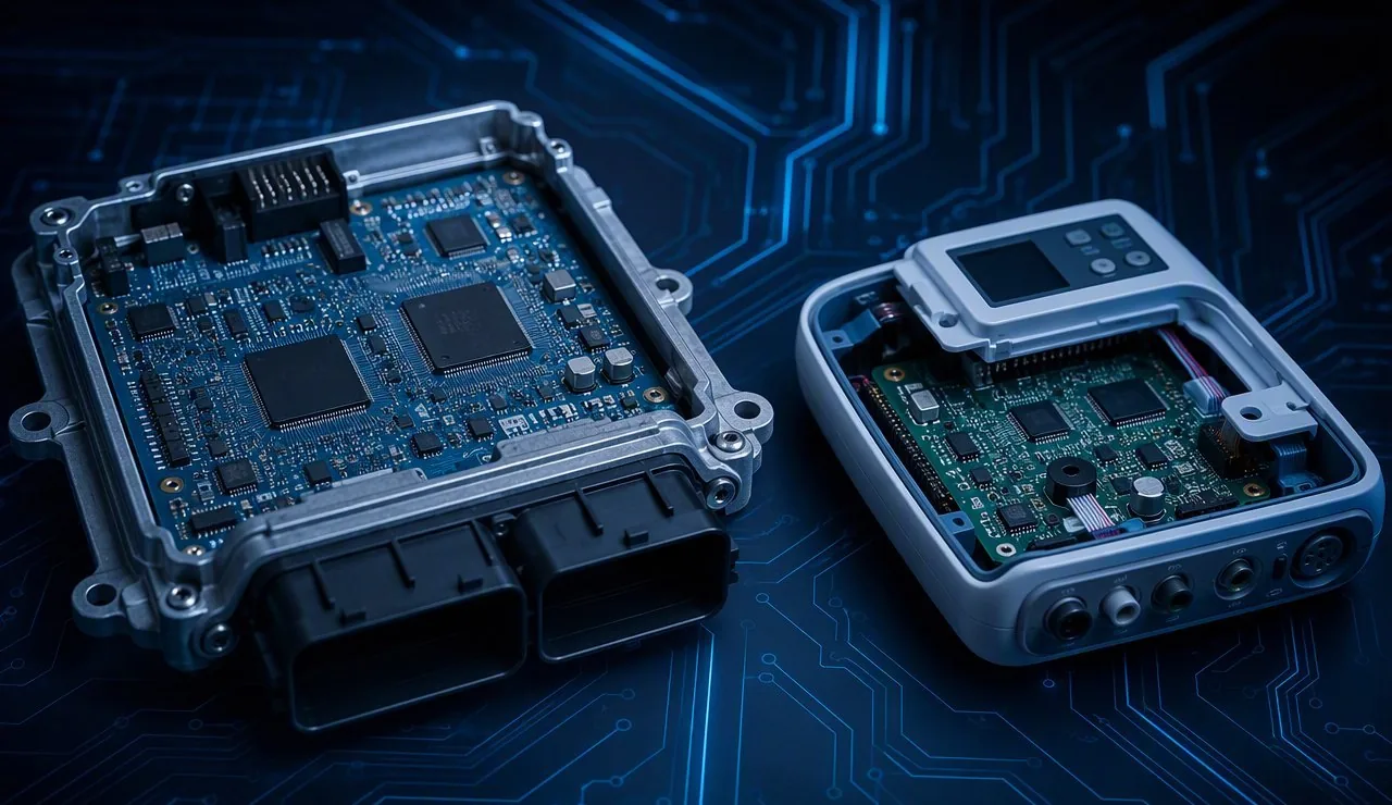
Define board fabrication, assembly, quality, and traceability requirements for the vehicle application.
Explore Industry Requirements
Coordinate fabrication and assembly for control, connectivity, sensing, and user-interface electronics.
Explore Industry Requirements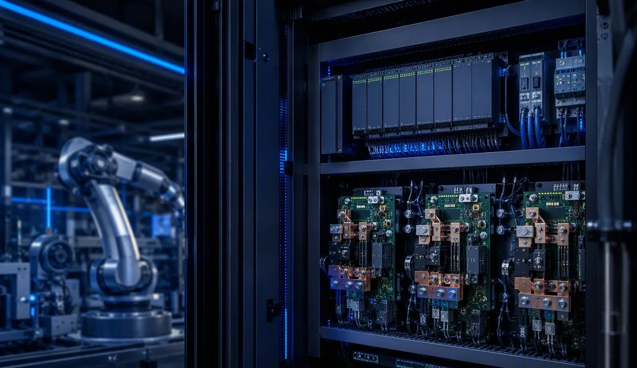
Review fabrication and assembly requirements for acquisition, communications, motion, and drive-control boards.
Explore Industry Requirements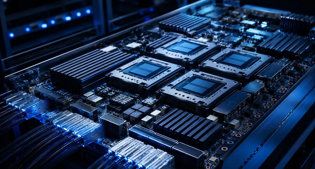
Discuss fabrication and assembly requirements for compute, control, power, and intelligent-device boards.
Explore Industry Requirements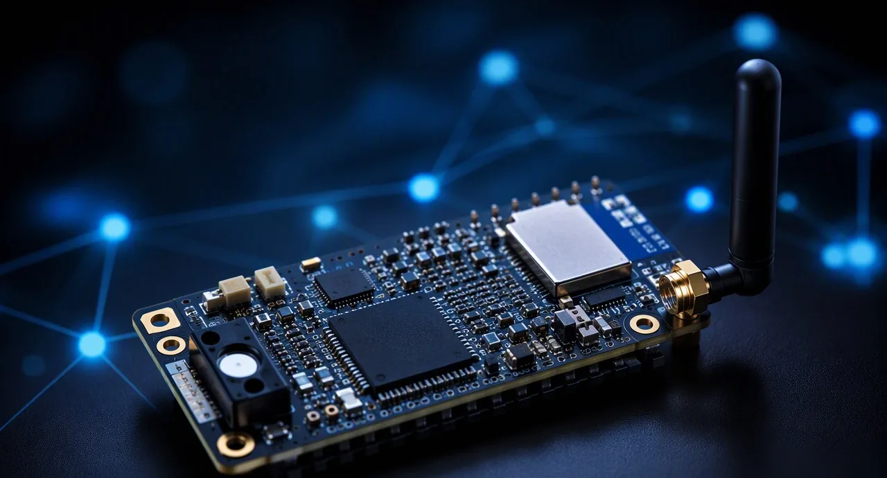
Coordinate board and module requirements from sensing nodes through connected edge devices.
Explore Industry Requirements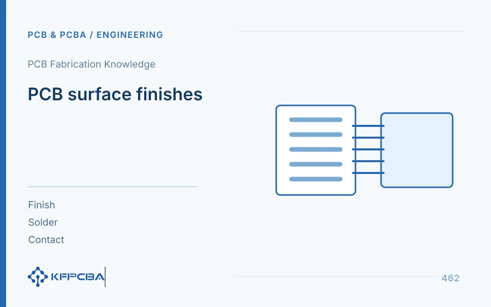
Select PCB surface finishes by region according to soldering, contact, and storage requirements. This article compares priorities for HASL, OSP, ENIG, immersion tin, immersion silver, and contact gold. A split-bag opening example explains inventory management, with records for coating-thickness definitions, region boundaries, and soldering-failure troubleshooting.
Read Article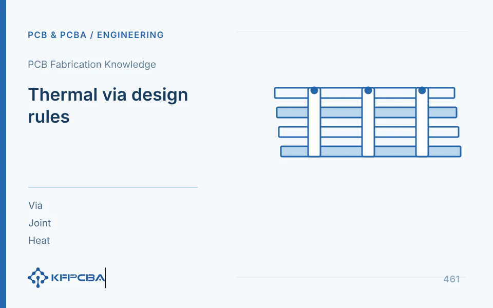
Thermal vias require joint review of hole-wall copper, fill, soldering, and external contact. This article uses hole-wall copper cross-sections and parallel thermal-path calculations to explain the limits of adding vias, with via-array configurations, stencil coordination, and measurement tables for diagnosing solder loss, voids, interface air gaps, and unchanged temperature rise.
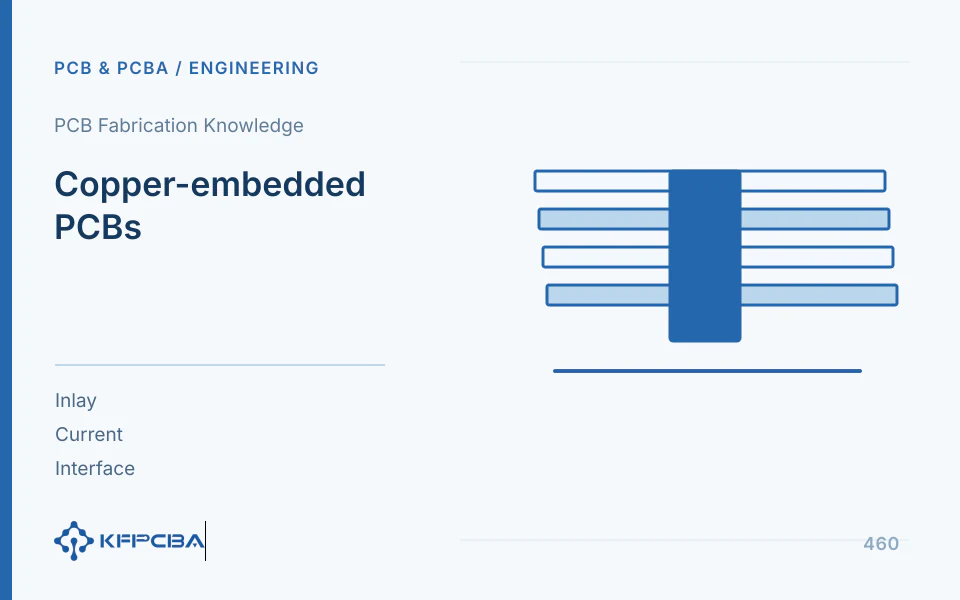
Embedded copper connects high-current or heat-transfer regions through local cross-sections; its capacity cannot be determined from copper weight alone. This article uses cross-section, resistance, and dissipation calculations to illustrate connection bottlenecks, and provides three-dimensional structural inputs, insulation and lamination checks, four-wire voltage-drop measurements, and local hot-spot troubleshooting.

Tell us the product use and which files are available. We can define the next engineering step even when the data package is not complete.