
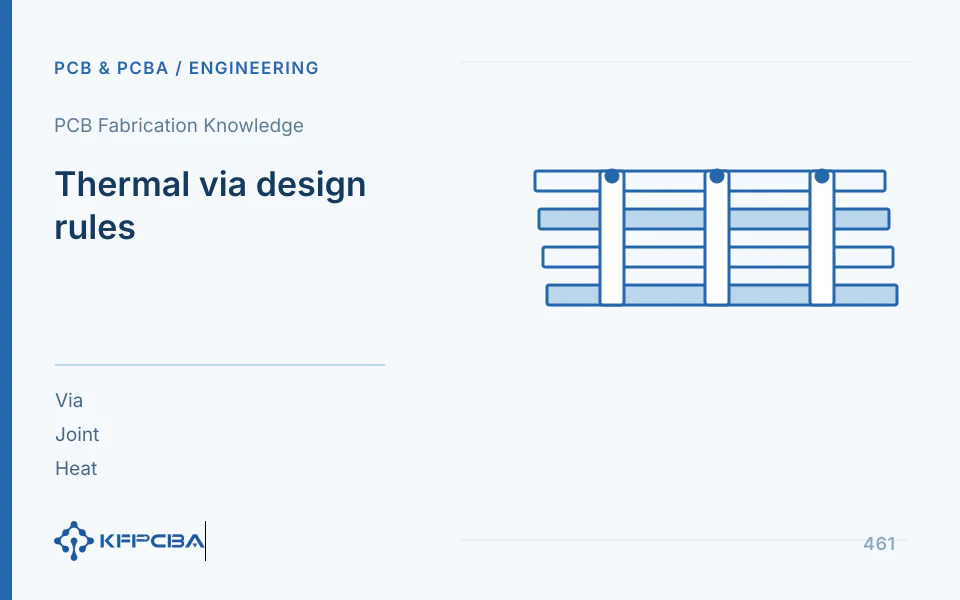
Thermal vias connect copper layers and heat-spreading regions through metal inside the holes. Their effectiveness depends on hole-wall copper cross-section, depth, quantity, surrounding copper spreading, and the final heat-removal path. Adding vias changes only part of that path. Vias under pads may also change solder flow and contact conditions, so thermal performance and assembly must be reviewed together.
First identify the thermal path connected by the vias
Draw the path section by section from the device thermal pad through top-layer copper, hole-wall copper, bottom-layer copper, interface material, and heat sink. If the bottom layer is only a small copper area with no effective heat-removal connection, vias may improve interlayer connectivity without providing an effective path to ambient. Also check the internal device-to-pad path; bottom-pad temperature cannot be treated directly as junction temperature.
Würth's Thermal Management design rules show both unfilled thermal vias and filled-and-capped constructions, illustrating that treatments suit different combinations. Example dimensions belong to that version of the supplier's rules and are not presented here as universal fabricator capabilities. Approve the actual via array against its stackup and intended use.
How to estimate hole-wall copper cross-sectional area
Assume a finished hole inside diameter D=0.30 mm and hole-wall copper thickness t=0.025 mm. The ideal wall cross-section is A=π[(D+2t)²-D²]/4=π(Dt+t²)≈0.0255 mm². For 16 identical vias, total wall area is approximately 0.408 mm². This calculation assumes ideal cylindrical walls and excludes nonuniform plating and connection regions.
One-dimensional axial conduction can be expressed as R=L/(kA). For ideal parallel vias of equal length and material, thermal resistance is approximately inversely proportional to via count. Actual vias share top and bottom spreading regions, however, and their heat flows interact. Solder joints and external interfaces also remain, so this does not predict whole-board temperature rise falling to 1/16. Resin fill is also not equivalent to adding copper conduction with the same cross-section.
A via-array specification needs more than diameter and count
| Configuration Items | Should Specify | Related Issues |
|---|---|---|
| Location | Via relationships to the device pad, copper regions, and heat sink | Solder release, heat dissipation, and contact |
| Geometry | Diameter definition, hole depth, pitch, and hole-wall copper | Thermal cross-section and manufacturability |
| Hole Treatment | Plated through hole, fill, copper cap, and side finish | Soldering and Surface Flatness |
| Copper and Interface | Copper area by layer, interface materials, and mounting | Whether Heat Exit Is Effective |
| Verification | Power consumption, measurement points, environment, and criteria | Results are repeatable and traceable |
The array must suit the actual device pad. Increasing via density until it compromises pads, traces, or process tolerances may create problems without significant benefit. Compare thermal effectiveness, assembly, and fabrication effort when selecting the construction.
Why can thermal vias cause solder loss and voids?
Open vias beneath pads provide solder-flow paths and change effective solder volume. Unevenness after covering or filling affects paste printing and component support. Solder voiding also depends on paste, stencil, thermal processing, and surfaces; visible voids alone do not prove there are too many vias. Review actual hole treatment, stencil apertures, and reflow records together.
Where a solderable plane is required, verify filling and capping rather than treating solder-mask tenting as the same construction. If the backside directly contacts a heat sink, hole openings, copper surfaces, and interface materials must also avoid air gaps or mechanical damage. Retest thermal performance after soldering changes, since altered contact can offset the benefit of additional hole-wall copper.
How to arrange joint first-article inspection
- Check that bare-PCB hole groups, fill, and surfaces match controlled drawings, and retain representative locations.
- Confirm stencil, solder-paste, placement, and reflow revisions, and record the actual assembly condition.
- Inspect agreed solder-joint and via-related conditions, supplementing with imaging and cross-sections when needed.
- Measure temperature under the same dissipation and mounting conditions, covering locations near the device, on the board backside, and on the heat sink.
- Link results to sample IDs, material lots, and assembly revisions, and make separate structural and thermal assessments.
Do not copy a void percentage from one application note as an acceptance limit for every device. Acceptable conditions and inspection methods must come from the specific device, thermal path, and product requirements. Test personnel should record the actual source of the criteria.
What should you check if more vias do not reduce temperature rise or make soldering worse?
| Phenomenon | What to Review First | What Evidence to Supplement |
|---|---|---|
| Temperature rise remains nearly unchanged | External contact, heat sink, and total power dissipation | Temperature Difference and Power per Section |
| Hot component with a cool board backside | Solder joints, thermal pads, and hole-wall copper connections | Soldering images, cross-sections, and hole conditions |
| Solder Balls or Solder Suction on Backside | Drill holes, side, and paste printing | Photos before and after assembly and hole processing records |
| Large difference after disassembly and reassembly | Flatness, fastening, and interface materials | Contact footprint and repeat assembly |
If bare metal reads unusually low in an infrared image, first rule out reflections and emissivity effects. Thermocouple attachment location and adhesive thickness also affect results. Only data for the same measurement object and boundary conditions can evaluate the benefit of adding vias.
How to compare plated holes and filled hole caps
When comparing the same via array, hold dissipation, copper area, heat sink, and mounting constant, recording fabricated surfaces, soldering results, and thermal response separately. Filling and capping may improve the assembly plane, but their cost, interfaces, and thermal paths also require evaluation. An open-via design outside a pad should not be rejected in advance if it meets the application requirements.
When comparing with copper-filled microvias, specify materials and hole types rather than describing them only as 'solid' and 'hollow.' Layer sequence, hole depth, fabrication, and intended use jointly determine feasible constructions. No calculation replaces representative samples and necessary reliability validation.
How can repeat orders preserve thermal-construction consistency?
Freeze the via array, hole-wall copper requirements, plugging/filling/capping, copper regions, and external interfaces. Changes to the stencil, device, or heat sink may alter soldering and temperature rise even when bare-board vias are unchanged; review according to their effects. Retain inputs, structural results, and thermal results separately so future anomalies can be traced to vias, solder joints, or mounting changes.
Update the fabrication drawing and hole table with the final hole treatment rather than applying a different covering as an assembly-floor workaround. Retain historical records for validated combinations. Outside that scope, define the additional tests needed instead of repeating unrelated checks.
How should thermal-path improvements be compared with solder deposition?
If the stencil or solder paste changes when thermal vias are added, thermal results may reflect several factors. Record stencil thickness, apertures, paste, and printing condition for comparison samples, and retain solder-joint images. A change in via count alone does not justify attributing every improvement or deterioration in temperature rise to hole-wall copper.
Reduced solder-joint contact area may increase device-to-board thermal resistance, which improved via conduction may not offset. Inspect the soldering interface first, then examine the temperature difference between the board backside and heat sink. This identifies the thermal-path segment actually affected by the via change and avoids further undirected increases in via count.
Retain evidence of manufactured via fill and capping before assembly. Depressions, solder balls, or voids appearing after assembly can then be compared with the original condition. Without pre-assembly records, bare-board surfaces are difficult to distinguish from soldering effects. Keep representative locations and sample IDs consistent across both stages.
Repeated removal and installation of a sample also changes interface-material thickness and fastening. List these operations separately in thermal testing and use repeated assembly to assess variation when needed. Discuss design benefits only when changes clearly exceed the method's own variability and the construction remains consistent.
Frequently asked questions
Can resin-filled holes serve as copper-filled holes?
Fill materials and heat paths differ, so they cannot be calculated using the same cross-section or performance assumptions.
Is denser hole spacing always better
Heat spreading, soldering, and fabrication constraints also apply. See Hole Treatment, Thermal Path Selection, Manufacturing Combination and Document List.
Source material and applicable scope
- Würth Elektronik, Design Rules Thermal Management; version: Version 1.2 / 11.2021 / 503637 EN; checked 2026-10-17; relevant sections: unfilled thermal vias, filled-and-capped vias, thermal simulations, and construction drawings; scope: supports differences between thermal vias and their treatments. Tube-wall cross-section and thermal-path calculations are ideal engineering examples; example dimensions are not universal rules.
