Plan multilayer PCB design for acquisition, industrial Ethernet and current-loop circuits. Define reference planes, isolation, clocks and calibration needs.
Multilayer PCB design: sampling, industrial controllers, and isolation
Compare eight-channel simultaneous acquisition, Ethernet controllers, and four-channel current loops; design reference planes, analog error budgets, isolation boundaries, and data paths, and validate prototypes by function. Multichannel acquisition and industrial controllers need continuous reference planes and clear functional partitioning; multilayer approaches also consider analog noise, interface return paths, and power distribution.
Configurations in this category support development requirements discussions. Actual components, structures, and performance are confirmed in the project revision; historical development directions and engineering references are identified separately.
How is multilayer PCB design priced, and what does the quotation include?
This category covers simultaneous acquisition, industrial Ethernet, and current loops. Costs are broken down by schematic, PCB layout, agreed software, and prototype validation scope; the main workload differences involve error budgets, layer order, interface protection, and synchronization/communication validation. Layer count, board area, or channel count alone cannot determine development pricing; the usability of existing files and test conditions also affect the effort.
Quotation terms depend on the approved files, quantity, material supply, tests and delivery requirements.
Implement layout using approved schematics, footprints, and mechanical design
Whether schematic review, stackup/constraints, and fabrication files are included
From functional R&D
Error budgets, layer order, interface protection, and synchronization/communication validation
Whether circuits, firmware, and validation targets are complete
Prototypes and revisions
Build prototypes from the frozen design, record test feedback, and release a controlled revision
Whether prototype quantity, component procurement, and change scope use the same basis
How should I choose between four-layer and higher-layer-count PCB designs?
Arrange sampling, power, reference planes, and interfaces first, then check routing density. More layers can improve layout space but add fabrication cost; structures that meet return-path and isolation requirements provide a valid basis for comparing total costs.
Start selection with channels, bandwidth, reference planes, and isolation boundaries, then review the parameters, cost boundaries, and validation conditions of the specific designs below.
Comparing approaches for sampling, industrial controllers, and isolation
Review Questions
Why it impacts design
How to select and close
Layer count and reference plane
Routing density, reference planes, and power integrity jointly determine layer count.
Assign adjacent reference planes to critical layers, and prevent high-speed and analog signals from crossing plane gaps.
Analog and digital
Switching return currents from digital processing and interfaces may enter the acquisition front end.
Partition functional regions by signal flow and control return paths and clock placement, rather than arbitrarily splitting every ground.
Interfaces and protection
Long-cable industrial interfaces need port protection, grounding, and isolation strategies.
Include cables, enclosure, shield connections, and test conditions in schematic and mechanical reviews.
Multi-layer PCB design order input
Acquisition channels, measurement range and bandwidth, interface rate, synchronization clock, power rails, isolation requirements, and mechanical interfaces.
Current Stage
Customer-Supplied Materials
Design deliverables
Functional requirements only
Acquisition channels, measurement range and bandwidth, interface rate, synchronization clock, power rails, isolation requirements, and mechanical interfaces.
Functional/state requirements, approach comparison, mechanical design, and open items for sampling, industrial controllers, and isolation
Existing schematics or PCB
Editable circuit/PCB files, BOM, and mechanical design for products in this category; include acquisition channels, measurement range and bandwidth, interface rate, synchronization clock, power rails, isolation requirements, and mechanical interfaces.
Functional partitioning, stackup and reference-plane descriptions, analog error budget, and interface test package
Existing prototype pending revision
Fault reproduction conditions, raw logs/waveforms, test equipment, and original board revision
Troubleshoot faults related to sampling, industrial controllers, and isolation, and deliver revised files, an impact list, and regression records under the same operating conditions
For low-frequency process-variable monitoring, simultaneous ΔΣ ADCs simplify multichannel synchronization; for higher bandwidth, switch to high-speed ADCs rather than only increasing serial-port speed.
MCU controllers suit deterministic acquisition and limited user interfaces; switch processor/core-board architecture when Linux applications or graphical interfaces are required.
Do not conflate a basic four-channel shared-ground design with per-channel isolation. Compare per-channel isolation costs for sites with significant ground-potential differences.
Manufacturing coordination and design delivery
Functional partitioning, stackup and reference-plane descriptions, analog error budget, and interface test package. Link deliverables to the same requirements revision; the PCB fabricator confirms materials, stackup, holes, and fabrication conditions, while PCB assembly checks footprints, soldering, programming, and test points. Recheck this category's constraints after critical-component substitutions or mechanical changes.
Multi-layer PCB prototype acceptance
Key validation in this category: acquisition error and crosstalk, clock synchronization, continuous data transmission, interface faults, and power-supply temperature rise.
Acceptance Stage
Conditions to be frozen
Report Records
Functionality and boundaries
Component/software revisions, supply/load, and interface or mechanical operating conditions
Test procedures, raw logs/waveforms, results, and abnormal states
Application-specific performance
Acquisition error and crosstalk, clock synchronization, continuous data transmission, interface faults, and power-supply temperature rise
Instruments and calibration, environment, samples, criteria, and exclusions
Version Closure
Change list, permitted limitations, passed items, and open items
Fabrication and software packages, test reports, and issue-closure records
Common questions on purchasing and customization
How should I choose between four-layer and higher-layer-count PCB designs?
Arrange sampling, power, reference planes, and interfaces first, then check routing density.
What should be established first when selecting multilayer PCB design?
First specify channels, bandwidth, reference planes, and isolation boundaries.
Should I commission only multilayer PCB layout, or complete development?
Layout-only work can be discussed when usable schematics and component information exist. Starting from simultaneous acquisition, industrial Ethernet, or current-loop requirements requires selection and circuit design first. Itemize software, prototypes, and testing separately; do not treat layout fees as a complete development budget.
How should a multilayer development budget distinguish the three acquisition/control approaches?
Itemize front end/clock/upload for eight-channel simultaneous acquisition, PHY/I/O/concurrent control for industrial Ethernet, and wiring/isolation/per-channel calibration for current loops. Separate shared layout work from application-specific software tests. Even for the same six- or four-layer construction, board area and channel count cannot replace work-package comparisons.
How should multilayer layout and front-end design responsibilities be divided?
Stackup and routing can be commissioned when the customer provides approved schematics, component models, measurement ranges, and interface constraints. Complete circuit review first if sampling common mode, protection, error budgets, or isolation are unresolved. Continuous reference planes address return paths but cannot replace analog-input adaptation or protocol definition.
How can multilayer industrial-control quotations avoid omitting data software?
Simultaneous acquisition needs sequence numbers/buffering and export, network control needs queues/rollback, and current loops need calibration coefficients and diagnostic codes. Even with existing customer host software, define board-side formats, error recovery, and integrated debugging; interface communication alone does not establish complete continuous-data or control functions.
What partitioning rationale should accompany multilayer source-file delivery?
Deliver the actual stackup, reference planes, net constraints, power and protection, isolation barriers, and editable circuit/PCB files. Retain raw logs and calibration revisions in reports for synchronization, control, or current error, so return paths and budgets can be checked when adding interfaces later; partitioning images alone are insufficient.
How should total development effort be compared when reducing multilayer board layers?
First validate breakout, analog noise, return paths, and power integrity, and compare whether the new stackup retains critical functions. Reducing layers adds layout and prototype regression work; calculate fabrication savings separately from one-time development costs. Decide only if constraints remain satisfied, rather than relying on board price alone.
Can acquisition and control functions reuse the same multilayer mainboard?
Check whether ADCs, real-time tasks, buffering, and field isolation all meet requirements concurrently. Identify reusable controller and upload modules, and separately review the analog front end and concurrent-operation noise; an industrial Ethernet mainboard's I/O count does not prove simultaneous precision acquisition capability.
How should I prepare an RFQ before commissioning multilayer PCB design?
Initially describe the product task, application, and current files. A formal quotation should confirm acquisition channels, measurement range and bandwidth, interface rate, synchronization clock, power rails, isolation requirements, and mechanical interfaces. If source files exist, provide circuit/PCB/BOM and mechanical revisions together; if prototypes exist, include fault conditions. First identify frozen functions and structures, then compare circuit, layout, software, and validation work; unresolved items must not be assumed to share the same service scope.
How should I compare multilayer PCB design prototype validation costs by operating condition?
Key validation in this category: acquisition error and crosstalk, clock synchronization, continuous data transmission, interface faults, and power-supply temperature rise. For each RFQ item, specify the actual load/interface or structure, prototype quantity, measurement method, equipment, and permitted deviation; deliver raw results, anomalies, and revision closure separately. Circuit/PCB checks and complete-unit functional validation are different tasks; a quotation including only the former does not justify omitting the performance measurements specific to this category.
Technical basis and applicable conditions
Select and place components using the manufacturer information in the specific design details, and record file revisions and applicable conditions with the project; the company's historical development directions do not mean the reference designs on this page have been delivered in volume.
Send the product functions, interfaces, mechanical constraints, available files, and required development stage. Compare design capability scope and development support before defining deliverables.
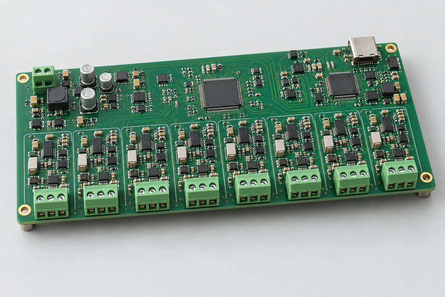
Eight-channel simultaneous acquisition board design: request separate quotations for eight front ends/error budgets, common clocks, SPI buffering/upload, and per-channel calibration. 8kSPS per channel is a reference target; align input ranges, storage formats, and upload endpoints when comparing quotations. PCB-only work cannot be compared directly with development including host calibration software.
Acquisition Channel
8 differential input reference requirements
Power Supply Objective
24V DC input; independent low-noise 3.3V analog domain
Stackup Candidate
6 layers; partition analog/digital by current loops
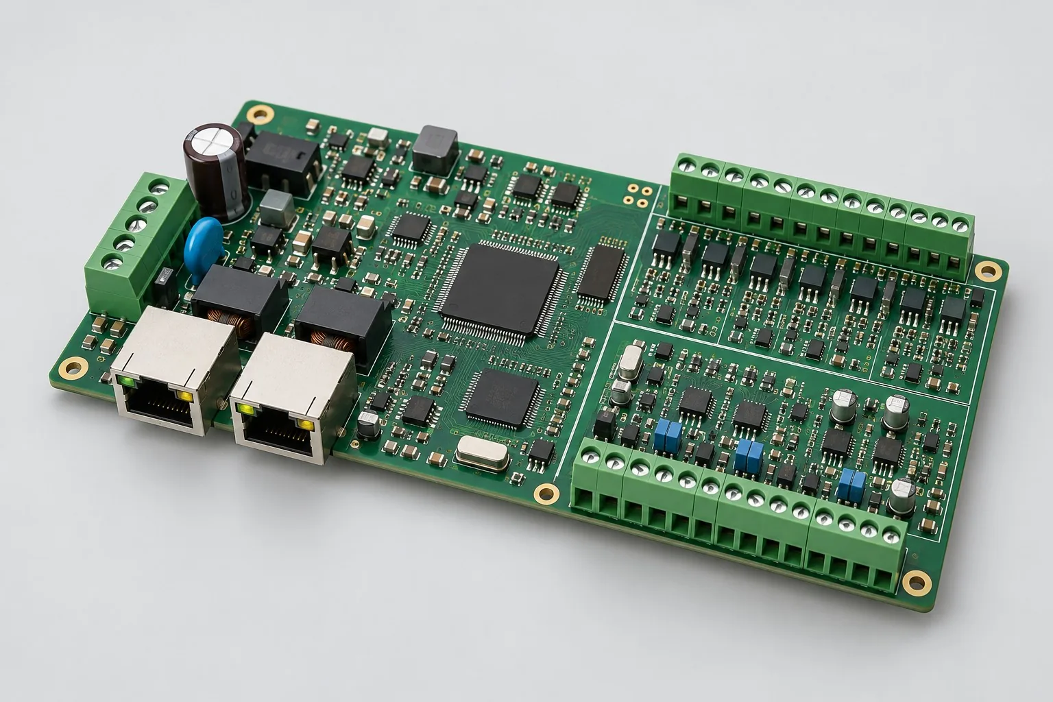
Industrial Ethernet control board design: list endpoints and tasks for reference 1-port 10/100M, 2-port RS485, optional CAN, and 8 inputs/4 outputs. Hardware includes input protection, PHY, and field I/O; software includes protocols, logs, and rollback. Quote network-saturated/concurrent-load prototypes separately rather than estimating all industrial development from one Ethernet port.
Finished Product Function
Equipment monitoring, data aggregation, control logic
Operating Input
24V DC nominal, input surge/reverse-polarity protection
Stackup Candidate
6 layers, continuous ground and separate power-distribution layers
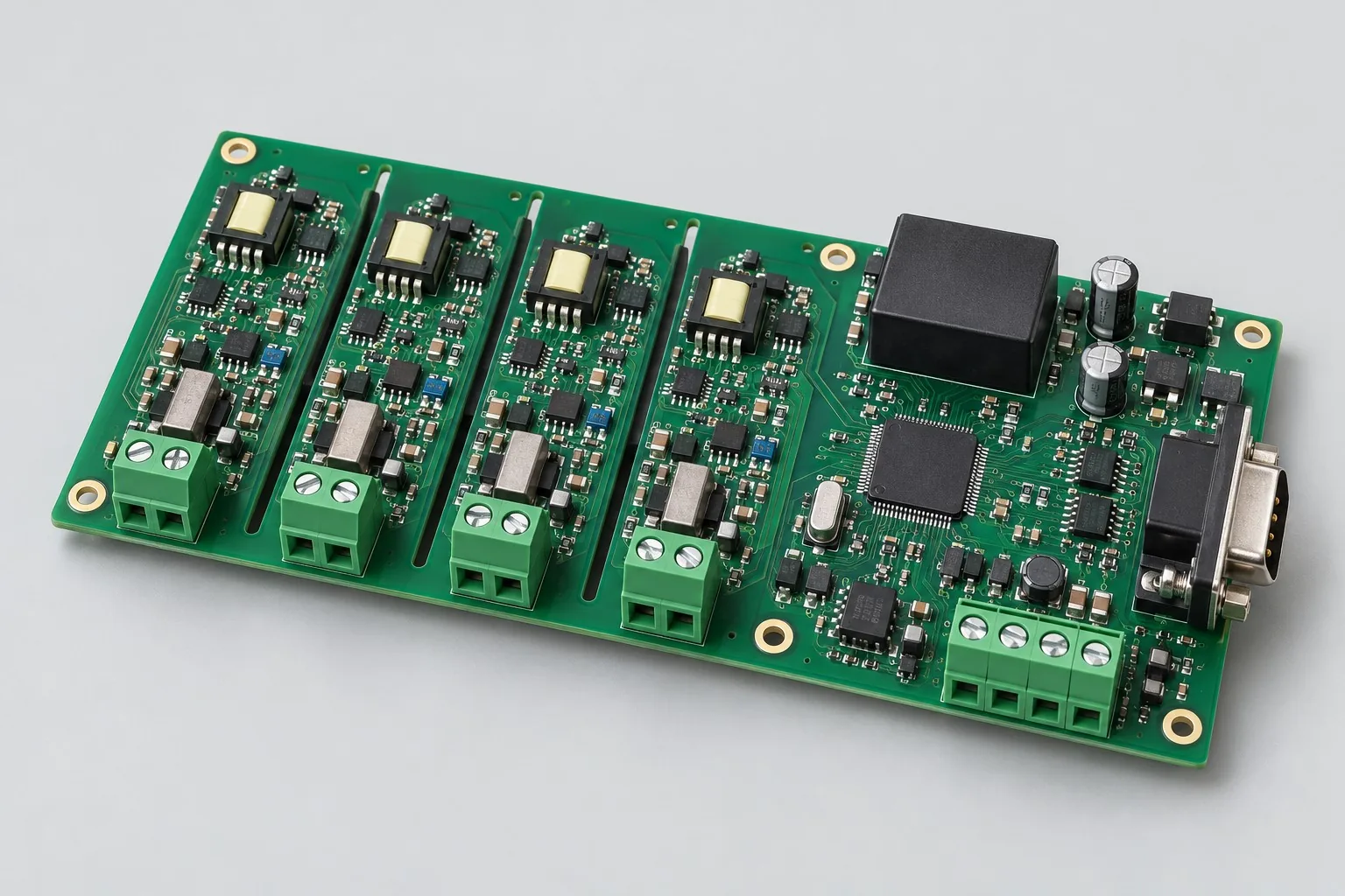
Define a four-channel 4–20 mA acquisition board around transmitter wiring, loop headroom, input errors, and field ground potentials. Compare shared-ground sensing with per-channel isolation, and specify calibration, diagnostics, and communication.
Reference Function
Four-channel 4–20 mA transmitter acquisition
Power Target
24V field input; budget sensor supply separately
Stackup Candidate
Four layers; field-side and controller-side isolation barrier defined
Communication Interface
Isolated RS485, optional Modbus RTU
Channel Structure
Four shared-ground low-side shunts + digital isolation; assess channel isolation separately