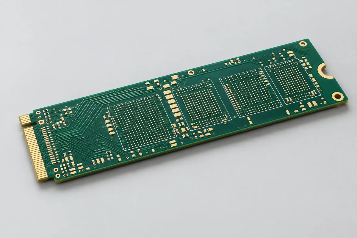
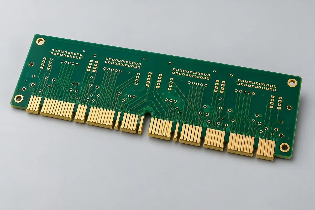
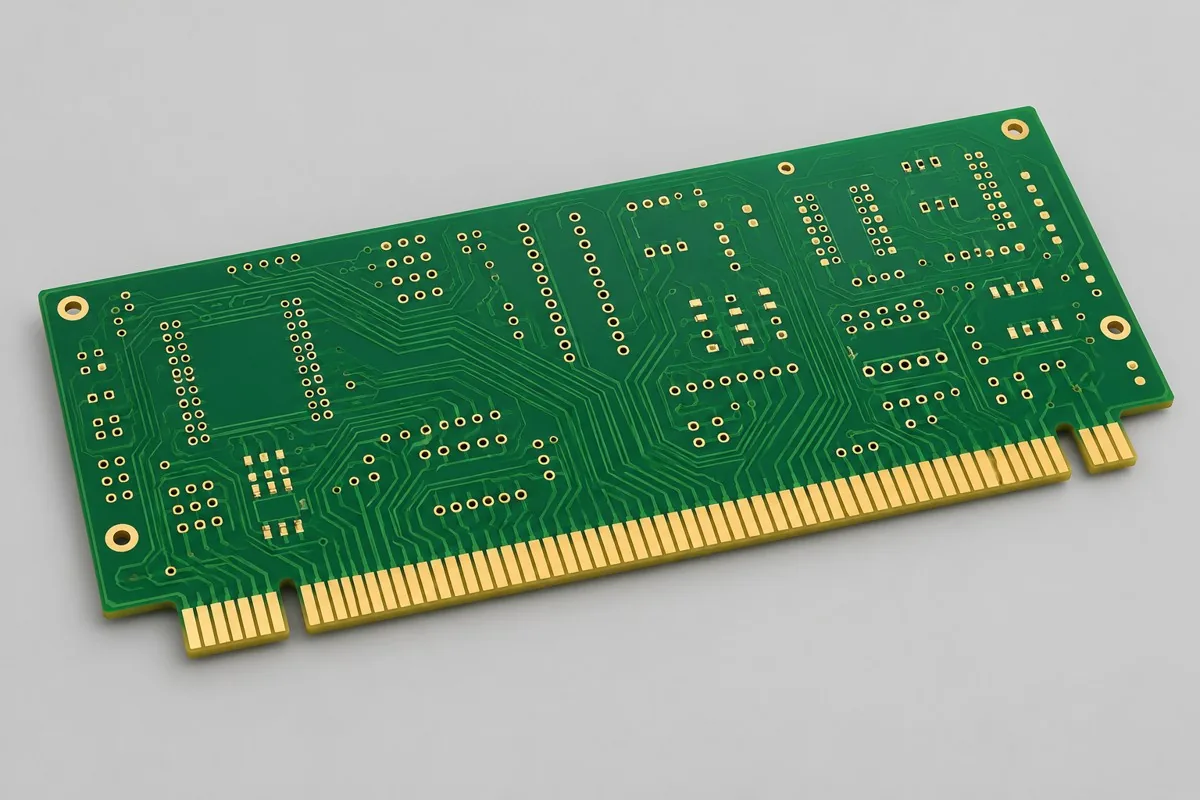
Gold-finger PCB fabrication: hard-gold contacts and slot datums
Gold-finger bare-board fabrication requires mating slots, contact lengths, key positions, bevels, and plating drawings. Review durability, contact sequence, and links separately for industrial cards, graded-contact test boards, and M.2. Deliver board-edge dimensions and nickel/gold records; thickness or plating alone does not guarantee mating life.
Convert Slot Drawing to Manufacturing Reference
Provide key positions, bevels, contact lengths, gold-finger areas, and plating requirements. Artwork, plating, and profiling must share the same mechanical datum; contact continuity does not establish contact sequence or mating durability.
Gold finger order: slot and plating map
After selecting a product in this category, submit mating slots, board-edge thickness, key positions, bevels, contact lengths, and plating. Match each change to the Engineering Reference Configuration, using the same revision for fabrication drawings, inspection locations, and material approvals; define specialized verification and report scope before quotation.
Back to all PCB products · Manufacturing file knowledge
Material and Process Reference
Consult selected PCB configuration
How do hard-gold fingers differ from ENIG PCBs?
Hard-gold contact applications differ from ENIG soldering-surface requirements; both being gold does not establish substitutability. Industrial cards, graded-contact test boards, and M.2 interfaces have different mechanical datums and contact sequences.
How should board thickness, bevels, and contacts be selected for industrial cards and M.2 boards?
Match slots and mating requirements first, then determine board edges and contacts. More gold-plated area does not automatically improve overall system reliability; contact areas, structural fit, and corresponding verification are critical.
Gold-finger PCB pricing and selection FAQ
How much do gold-finger PCBs cost? Can hard gold and ENIG be substituted
A project-specific quotation requires review of the available files, quantity, materials, requested tests, delivery destination, taxes, shipping, and trade terms. This is not a complete finished-product quotation. Base fabrication/sample pricing, special processes, and inspections must not be billed twice. Any formula on this page organizes cost inputs; it is not a quoted rate.View cost items, calculation conditions, and sources.
How should I compare quotations from gold-finger PCB manufacturers?
Check contact-area nickel/gold coverage, slots, and bevels; quotes should match the connector. Gold-plated area or thickness alone cannot establish mating life; define mechanical and plating inspections separately.
Is it reasonable to calculate gold-finger plating costs using the whole board area?
Mark actual contact areas and plating scope before agreeing pricing and inspection criteria. More gold plating does not automatically increase system reliability; areas must match the slot.
Does equal board thickness guarantee compatibility with M.2 or industrial slots?
Also check key positions, bevels, pin sequence, and contact lengths against connector drawings. Similar outlines cannot replace mechanical and electrical compatibility checks.
Can a basic card designed for insertion while powered off be directly converted to hot-swap use?
Contact sequence is only part of the requirements; power current limiting, default signal states, and software recovery also matter. Review structural and system development separately; hard-gold surfaces do not establish live-insertion capability.
Which records must be rechecked when bevels change on a gold-finger repeat order?
Check slot fit, effective contact areas, and board-edge dimensions, synchronizing approved drawings and inspections. Plating records alone cannot establish continued fit after mechanical changes.
Consult Gold Finger PCB for Quotes: describe the application, existing configuration, and expected quantity so we can discuss bare-board fabrication requirements, inspection, and delivery conditions.
How much do gold-finger PCBs cost? Can hard gold and ENIG be substituted
Quotes should separately account for contact-area nickel/gold and area, board-edge thickness, bevels and key positions, contact lengths and sequence, and plating and mechanical inspections. List initial-order setup charges separately from per-batch and per-board charges; for equal quantities, also align revisions, delivery configurations, and tax and freight terms to identify whether price differences reflect configurations or excluded work.
Quotation terms depend on the approved files, quantity, material supply, tests and delivery requirements.
Prepare a structured RFQ or use the short inquiry form.