Why double-sided SMT costs more than single-sided SMT
Quotes should separately account for stencils and placement on both sides, second reflow and support, subsequent installation of heavy components, and communication or storage functional testing. List initial-order setup charges separately from per-batch and per-board charges; for equal quantities, also align revisions, delivery configurations, and tax and freight terms to identify whether price differences reflect configurations or excluded work.
Quotation terms depend on the approved files, quantity, material supply, tests and delivery requirements.
Prepare a structured RFQ or use the short inquiry form.
How should double-sided reflow and subsequent heavy-component installation be compared?
Double-sided assembly adds placement and thermal processes but provides more layout space. Whether heavy components can undergo second reflow, component heat limits allow it, and test points remain accessible all affect actual operations.
How should components and test points be arranged on double-sided communication and storage boards?
Communication boards require interface-position and reference-plane checks; recording boards require storage, power, and identity checks. Determine component groups on both sides and assembly height limits first, or later structural additions may change manufacturing and testing arrangements.
Double-sided PCB assembly: outsourcing and acceptance
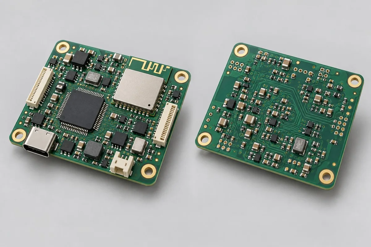
Double-sided PCB assembly describes component assembly on both sides and is reviewed separately from PCB layer count. Compact communication or recording boards require confirmation of both CPLs, reflow order, heavy-component retention, and support, with final functions verified after second reflow and subsequent installation.
Communication boards focus on modules/shielding/interfaces and reconnection; recording boards focus on ADC/storage/data during power loss. Both require first-side reinspection after second reflow.
Differences in assembly and test paths
Define reflow order, bottom-side support, and heavy-component retention first; test networks after subsequent soldering/shielding is complete, and measure sampling noise on recording boards during storage writes.
Double-sided compact communication control board
Bottom-side light components → top-side main-component reflow → subsequent interface/shield installation. Address first-side component displacement, bottom-side pressure damage, shield shorts, and identity errors separately. Retest interfaces after final shield installation; one-sided AOI or visual inspection does not represent the final double-sided condition.
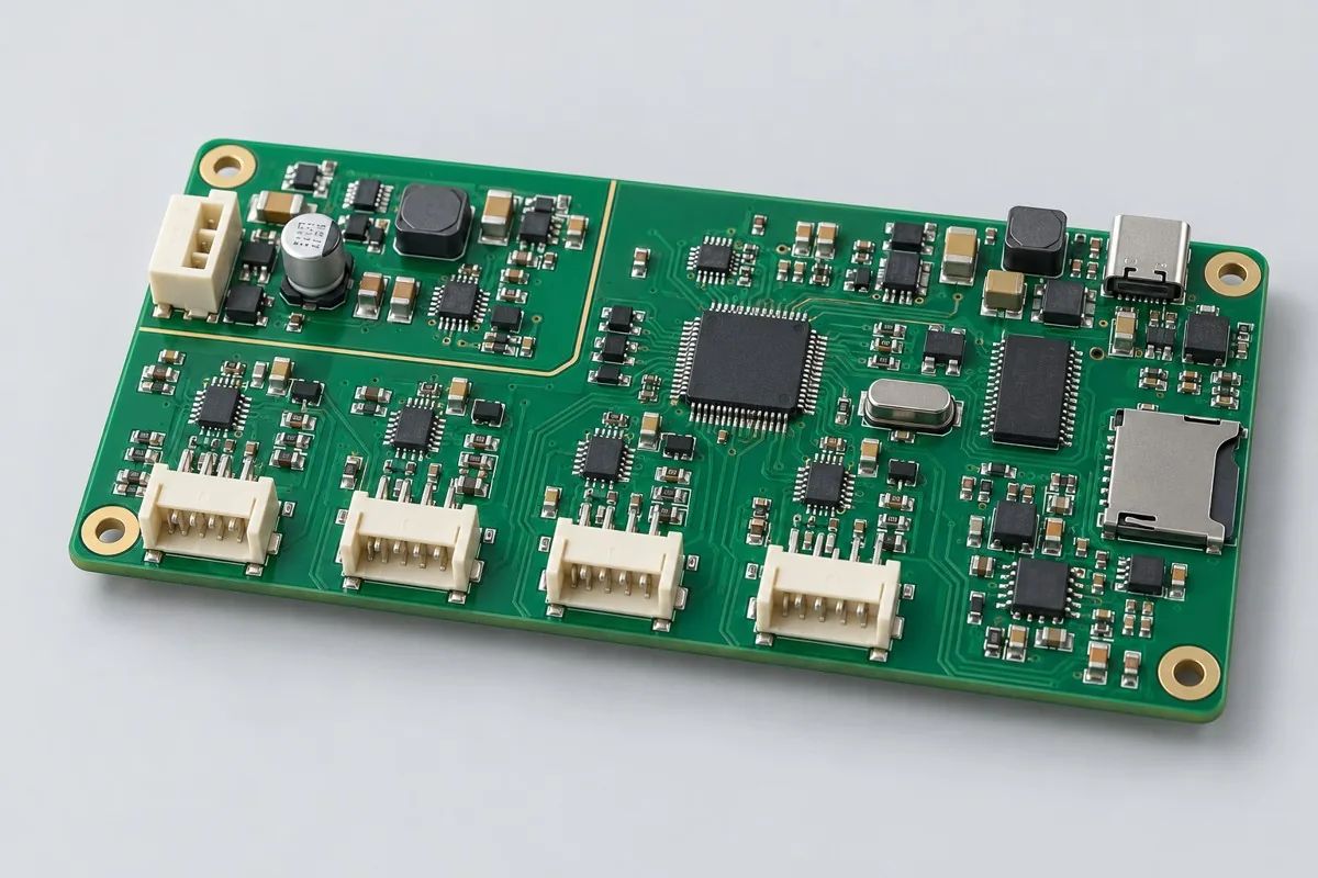
Double-sided sensor data recording board
Double-sided SMT → subsequent card-socket/socket installation → calibration → read/write testing. USB recognition cannot rule out channel misalignment, poor card-socket solder joints, corrupted files, or timestamp anomalies. Acceptance includes actual recording/readback and power-loss behavior; after rework, recheck sampling and storage working together.
Double-sided routing and actual condition testing
Provide component height limits for both sides, panel supports, and reflow-side order. Test concurrency and recovery on communication boards and power-loss files and low-power operation on recording boards; one communication-pass result cannot cover both. Assembly order: light/heavy components, heat tolerance on both sides, and retention conditions; do not assume all heavy components can be on the bottom. Supports and fixtures: warpage, tall bottom-side parts, carrier contact, and panelization; validate board entry and applied forces with the first article.
Component supply, quantity and delivery
Double-sided does not mean 2 layers; select and freeze revisions for PCB layer count, enclosure height, modules, and storage media separately.
For the order, align Gerber /BOM/CPL/DNP and assembly drawings, quantities, consigned/procured material lists, and firmware verification; costs and delivery include preparation for both sides, rework/retesting, firmware, and functional results, with scheduling confirmed from material readiness and actual labor time. Confirm stencil/carrier/fixture preparation, assembly operations, programming/calibration, and supporting tests on this page as separate charges. Agree replenishment/loss allowances, surplus materials, and inventory affected by changes in advance; list delivery milestones after material readiness and scheduling are confirmed. Regression-test component/interface/structure/firmware changes against the relevant tests, and record prototype issues separately from production release.
Material and Process Reference
Double-sided PCB assembly pricing and selection FAQ
Why double-sided SMT costs more than single-sided SMT
For standard placement, first calculate board quantity × billable points per board × price per point + setup fee. A project-specific quotation requires review of the available files, quantity, materials, requested tests, delivery destination, taxes, shipping, and trade terms. This is a placement-only reference; bare PCBs, materials, and testing are charged separately. Any formula on this page organizes cost inputs; it is not a quoted rate.View cost items, calculation conditions, and sources.
How should I compare quotations from double-sided PCB assembly suppliers?
First list the process order according to components on both sides and thermal limits, then check heavy components and height limits, and define communication and storage verification separately. Quotes listing only double-sided placement counts without second-reflow support and subsequent installation scope cannot reliably establish complete cost.
Does SMT on both sides mean the PCB has only two layers?
Double-sided refers to component assembly sides, not copper layers. Provide the actual stackup and component lists for both sides separately to avoid mixing double-sided reflow costs with two-layer PCB fabrication.
How should second reflow be confirmed when heavy components are on the bottom?
Check component weight, thermal limits, support, and process sequence to determine whether subsequent installation is needed. Equal placement counts on both sides do not imply identical routes or preparation.
Does a storage board need read/write retesting after its card socket is installed?
Verify storage, export, and power-loss recovery in the final card-socket and interface condition. Earlier power-up and solder-joint records do not cover the actual data path after subsequent installation.
Can I reuse one side's old stencil and remake only the other side?
Check pads, panel positioning, and apertures for each side separately, identifying the changed side and revision. List reuse conditions separately from this batch's feeder loading/first article; a minor board change does not waive preparation for both sides.
Consult double-sided PCB assembly quotation: describe the application, existing configuration, and expected quantity so we can discuss assembly inclusions and selection requirements.