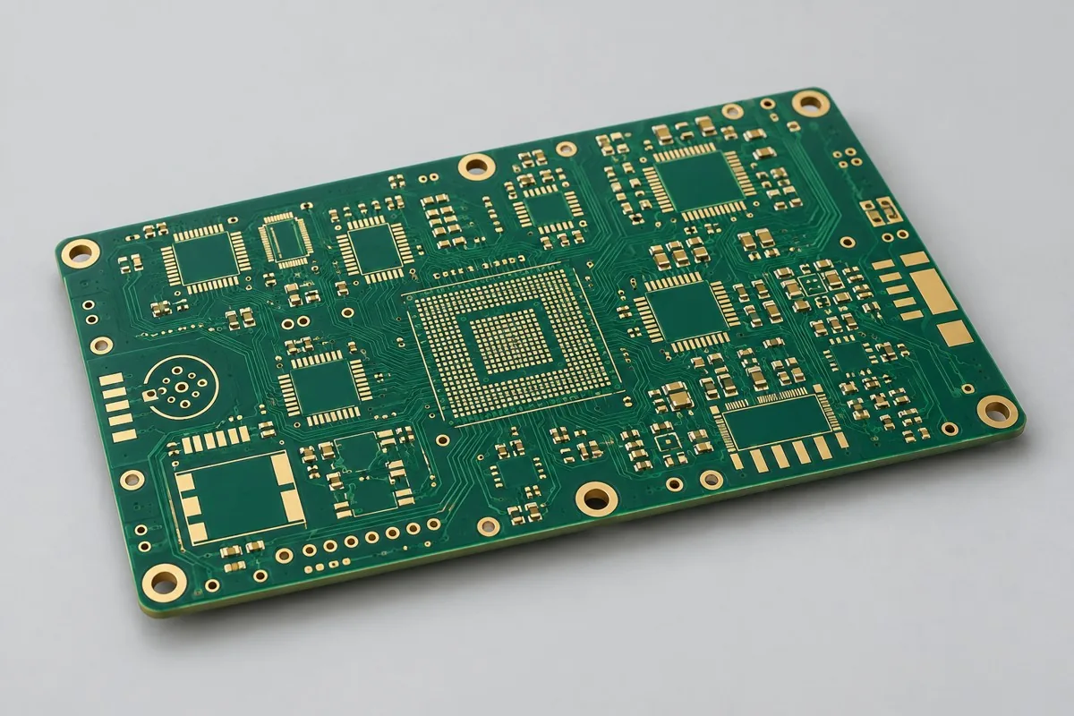
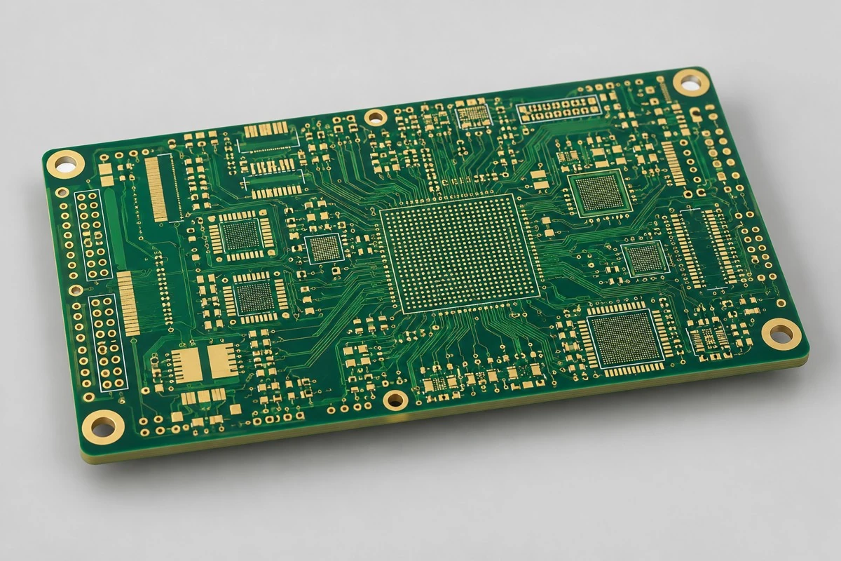
Compare HDI buildup routes, microvia layer pairs and fine-pitch breakout needs. Review stackup, via reliability and fabrication documentation together.
HDI PCB fabrication: package escape routing and via layer-pair review
For HDI bare-board fabrication, submit package pads, build-up dielectric thicknesses, and each build-up cycle's via layer pair. Use the lamination sequence to evaluate a one-build-up-layer-per-side structure, a two-build-up-layers-per-side staggered-microvia structure, or another approved HDI construction. Filled and copper-capped vias are not included by name alone; approve via drawings in the quote before agreeing microvia chains and microsections, keeping historical T-BOX hole sizes separate from new reference sizes.
HDI examples with one, two, or three build-up layers per side
The examples show one, two, or three build-up layers per side around a four-layer core: 1+4+1, 2+4+2, and 3+4+3. The approved stackup—not the label alone—defines the total copper-layer count. Process core buried vias first according to approved operations, then complete each build-up layer, blind microvias, and metallization. Staggered, stacked, and skip vias have different manufacturing conditions; hole diameters, positions, or connections in the drawings are not factory commitments.
Provide files for each lamination and drilling cycle for structures with one or two build-up layers per side; via filling, copper capping, and stacked vias are not included by default under the HDI label. Agreed microsection locations must cover all actual via structures, not just outermost microvias.
HDI fabrication: build-up layers, via layer pairs, and via filling
After selecting a product in this category, submit package pads, via layer pairs for each build-up cycle, build-up dielectric thickness, staggered-via coordinates, and filling scope. Match each change to the Engineering Reference Configuration, using the same revision for fabrication drawings, inspection locations, and material approvals; define specialized verification and report scope before quotation.
How does a one-build-up-layer-per-side HDI structure differ from a conventional through-hole multilayer board?
Conventional through-hole and HDI boards differ in connection density and interlayer connection routes. One-build-up-layer-per-side and more complex structures depend on specific stackups and via connections, not total layer count alone. Added fabrication steps change costs.
How should the build-up structure be selected for T-BOX and camera-processing boards?
Determine the need for microvias using component pitch, board outline, and escape-routing space first. Select interconnect structures separately for T-BOX, camera-processing, and one-build-up-layer-per-side examples; do not add unnecessary build-up layers merely to use the HDI label.
HDI PCB pricing and selection FAQ
Why does HDI prototyping cost more? How do one and two build-up layers per side differ?
A project-specific quotation requires review of the available files, quantity, materials, requested tests, delivery destination, taxes, shipping, and trade terms. This is not a complete finished-product quotation. Base fabrication/sample pricing, special processes, and inspections must not be billed twice. Any formula on this page organizes cost inputs; it is not a quoted rate.View cost items, calculation conditions, and sources.
How should I compare quotations from HDI PCB manufacturers?
Request via layer pairs and lamination routes, then examine via filling, fine traces, and microsections. Through-hole and HDI boards with equal layer counts use different operations; a cheaper structure that cannot support escape routing is not a substitute quotation.
Can a six-layer board be quoted directly as one-build-up-layer-per-side HDI?
Total copper-layer count does not define the number of build-up layers per side. Provide microvia/buried-via start and end layers and sequential lamination, and clarify via filling and fanout before confirming the manufacturing route.
Why should HDI filled vias, stacked vias, and staggered vias be quoted separately?
Via positions and connection sequence affect lamination and inspection; minimum hole size alone is insufficient. Complete via layer pairs and representative via chains ensure manufacturers quote the same structure.
If a one-build-up-layer-per-side HDI structure routes successfully, is there any reason to add another build-up layer per side just for the label?
First demonstrate that connections and space require an additional build-up layer per side; otherwise added operations may not add application value. Compare complete costs with the same board-outline and component constraints.
After HDI electrical testing passes, are microsections or post-stress retests still needed?
Representative via-chain geometry and stability differ from continuity. Agree samples, methods, and criteria according to project risks; one continuity pass cannot establish complex-microvia lifetime.
Consult HDI PCB quotation: describe the application, existing configuration, and expected quantity so we can discuss bare-board fabrication requirements, inspection, and delivery conditions.
Why does HDI prototyping cost more? How do one and two build-up layers per side differ?
Quotes should separately account for microvia layer pairs and formation processes, sequential lamination count, fine traces, via filling and fanout, and via-structure and microsection inspections. List initial-order setup charges separately from per-batch and per-board charges; for equal quantities, also align revisions, delivery configurations, and tax and freight terms to identify whether price differences reflect configurations or excluded work.
Quotation terms depend on the approved files, quantity, material supply, tests and delivery requirements.
Ten-layer camera HDI boards: review 2-6-2 staggered vias, processor fanout, copper-weight options, and interconnect tests. All values are illustrative; approve fabrication drawings and acceptance criteria before ordering. Assembly and system verification require separate scope.
Eight-layer T-BOX HDI boards: review 1-6-1 via layer pairs, package breakout, via filling, and representative microsections. All values are illustrative; approve fabrication drawings and acceptance criteria before ordering. Assembly and system verification require separate scope.
Material
TG170 History
Structure
8 Layer Single-Build-Up HDI
Specification
Historical information does not fully define materials and copper weight by layer. Current fabrication follows the approved material list and stackup.