Engineering Reference Configuration
RF transceiver board assembly: assembly configuration and test deliverables
The following adjustable engineering configurations support material, functional, and process review; they are not stocked models or commitments to current production-line capabilities. Approved fabrication documentation and order acceptance requirements govern.
RF transceiver board PCB assembly supports contract manufacturing and procurement review for RF transmission/reception, gain control, and baseband interfaces. First confirm transceiver + filtering/matching + optional power/low-noise amplifiers, SMA or board-edge RF ports, SPI control, baseband interfaces, and mixed RF-material/FR-4 construction or separate RF sub-boards. Then compare RF SMT → connector soldering → pre-shield inspection → link testing scope and acceptance costs for port matching, transmit/receive links, power consumption, and shielding effects. This page separates board + band configuration + calibration files + test records from order-specific band/power design parameters; it does not specify whole-board limits. This helps determine whether quotations cover the actual application. Quotation documentation reference:BOM · bare board · material supply
Reference specification and configuration options
| Options | Reference Configuration |
|---|---|
| Power and Logic Domains | 12V input; separate RF/digital power regions |
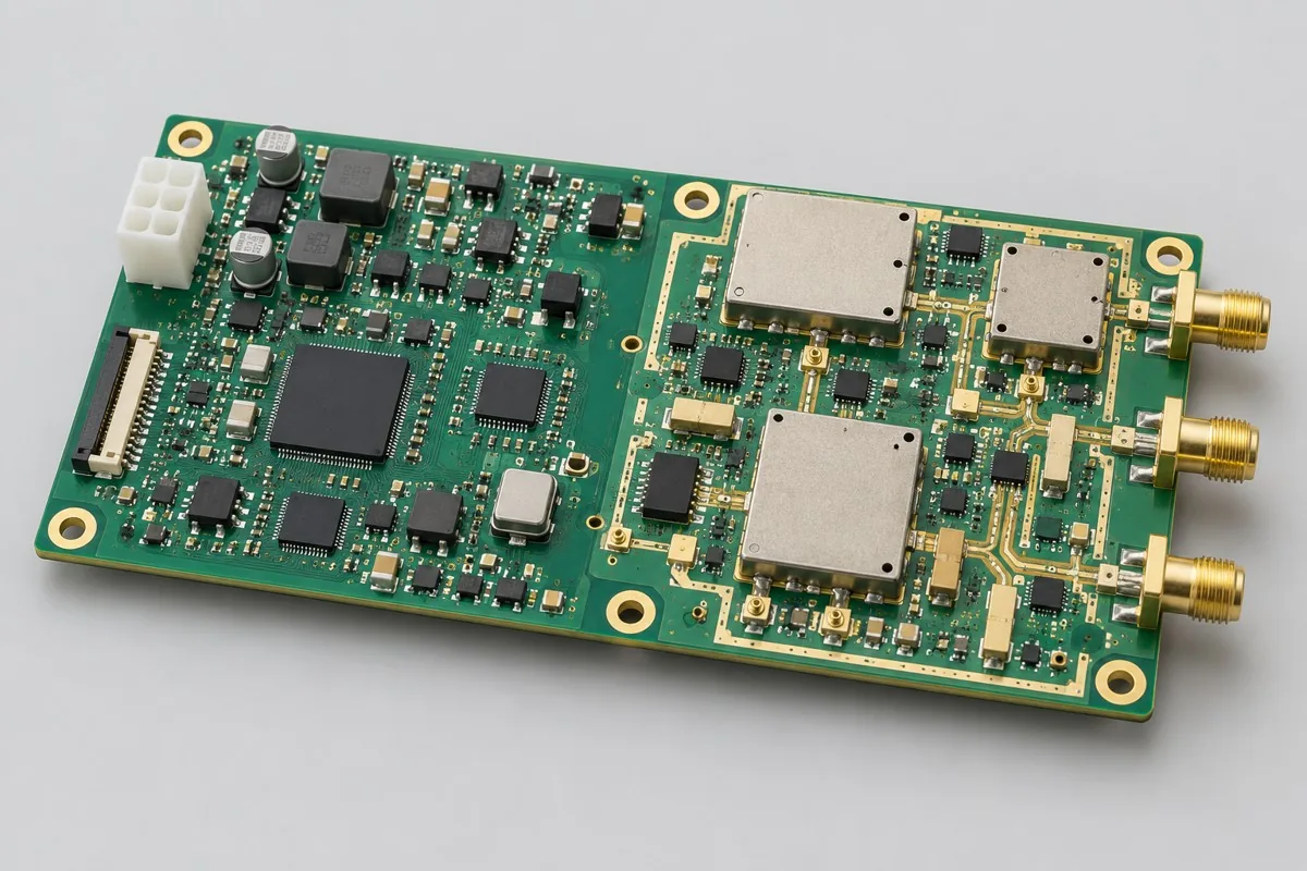
| Functional Module | RF transmission/reception, gain control, and baseband interfaces |
| Core Components/Architecture | Transceiver + filtering/matching + optional power/low-noise amplifiers |
| Interface and Channels | SMA or board-edge RF ports; SPI control; baseband interfaces |
| Board Layers and Material Options | Mixed RF-material/FR-4 construction or separate RF sub-boards |
| Component packages | QFN RF ICs, matching passives, shielding cans, coaxial connectors |
| Assembly Route | RF SMT → connector soldering → pre-shield inspection → link testing |
| Material Supply Scope | Specified RF ICs and matching components; coaxial accessory models locked |
| Firmware and Parameters | Band/gain tables, calibration data, and control firmware |
| Test Focus | Port matching, transmit/receive links, power consumption, and shielding effects |
| Deliverables | Board + band configuration + calibration files + test records |
| Configuration Limits/Options | Band/power are order-specific design parameters; this page does not specify whole-board limits |
How much does RF transceiver board PCB assembly cost, and what is included?
RF ICs, filtering/matching components, coaxial connectors, and optional power/low-noise amplifiers are major costs. Pre-shield inspection, connector assembly, link calibration, and band-specific tests cannot be priced solely by SMT placement counts. Test cables, fixtures, and calibration planes also affect setup. Compare designs with different power levels, bands, or shielding structures separately.
Quotation terms depend on the approved files, quantity, material supply, tests and delivery requirements.
Prepare a structured RFQ or use the short inquiry form.
| Cost Item | Scope for This Configuration | Billing frequency and work scope | Procurement Verification |
|---|---|---|---|
| Bare PCB and core components | Transceiver + filtering/matching + optional power/low-noise amplifiers; mixed RF-material/FR-4 construction or separate RF sub-boards | Price according to actual bare-board/component purchase quantities; authorize critical components and substitutions individually | Specified RF ICs and matching components; coaxial accessory models locked |
| Placement and secondary assembly | RF SMT → connector soldering → pre-shield inspection → link testing | Feeder/program setup per lot; assembly priced per board, joint, or process as agreed, with counting rules specified | QFN RF ICs, matching passives, shielding cans, coaxial connectors |
| Manufacturing Preparation | Review stencils, first articles, and support tooling against the actual assembly route | New stencils/carriers may be separate one-time charges; verify panelization, revision, and condition before reuse | Reduced quantities do not automatically eliminate first-article or feeder setup |
| Test resources and execution | Port matching, transmit/receive links, power consumption, and shielding effects | Itemize test-method/fixture/script setup; agree execution charges per board, channel, or test duration | Separate supporting development from execution records for each board |
| Software and Parameters | Band/gain tables, calibration data, and control firmware | When firmware exists, distinguish file programming/verification from software development; omit programming without a firmware revision | Customer-approved files, parameters, and readback rules determine scope |
| Delivery and Change | Board + band configuration + calibration files + test records; band/power are order-specific design parameters; this page does not specify whole-board limits | Price accessories, retesting, and revision changes by approved work items; do not prefill fixed rates | Check BOM, tooling, programs, and acceptance revisions before reorders |
How should separate RF modules and combined RF/digital boards be selected?
Separate modules simplify sectional testing and model changes but add connection loss and height. Combined boards reduce interfaces while requiring RF, digital, and thermal paths to be handled together. Compare mechanical space, target links, and maintenance needs before total costs.
| Comparison Metric | Current Conditions | Factors Influencing Procurement Decision |
|---|---|---|
| Manufacturing Delivery | RF SMT → connector soldering → pre-shield inspection → link testing | Produce boards/assemblies per BOM and assembly drawings; this does not establish that every system function passes |
| Functional Acceptance | Port matching, transmit/receive links, power consumption, and shielding effects | Compare unit prices after defining test stimuli, limits, accessories, and records; review missing test inputs first |
| Configuration Options | SMA or board-edge RF ports; SPI control; baseband interfaces; mixed RF-material/FR-4 construction or separate RF sub-boards | Confirm circuit/program compatibility before reviewing assembly and test costs for interface, stackup, or component changes |
| Delivery Scope | Band/power are order-specific design parameters; this page does not specify whole-board limits | Complete-system accessories, application development, and project verification are not automatically included in board assembly |
Can RF matching capacitors be replaced with cheaper parts of equal capacitance?
Equal capacitance does not mean equal high-frequency behavior; check packages, parasitics, frequency characteristics, and actual pads. Reverify links at identical calibration planes after substitutions; compare procurement savings with verification costs and subsequent risks.
- First list required RF transmission/reception, gain control, and baseband interfaces, distinguishing build-to-print manufacturing, configuration adjustments, and new-function development.
- Then freeze complete part numbers for transceiver + filtering/matching + optional power/low-noise amplifiers, SMA or board-edge RF ports, SPI control, baseband interfaces, and mixed RF-material/FR-4 construction or separate RF sub-boards. Separate customer-supplied and sourced materials with RF ICs/matching components specified and coaxial accessory models locked.
- Use first articles to check RF SMT → connector soldering → pre-shield inspection → link testing, plus band/gain tables, calibration data, and control firmware. If only program files are supplied, agree programming verification first; development requires separate review.
- Convert port matching, transmit/receive links, power consumption, and shielding effects into acceptance items with stimuli, limits, and records; specify fixture ownership, per-board execution, and post-repair retesting.
- Finally confirm board + band configuration + calibration files + test records. Band/power are order-specific design parameters; this page does not specify whole-board limits. Compare totals using identical quantities, accessories, and test scope, then freeze the order revision.
Applicable uses and situations requiring separate review
RF transceiver subsystems, wireless measurement interfaces, RF link verification.
Without frequency bands and link budgets, do not start procurement from generic BOMs. Multiband RF products cannot claim compatibility by changing one filter alone. Ordinary low-speed digital boards do not require hybrid RF-material stackups.
Assembly Challenges for This Product
Tiny matching-component values, locations, and solder shapes affect RF paths. Complete component-value and joint checks before installing shields; prevent stress on center pins after connector soldering. Fix test cables, calibration planes, and connection torque.
Structural, thermal, and configuration trade-offs
Mixed materials can confine specialty laminate to the RF regions but introduce different lamination, soldering, and rework conditions. Separate RF modules simplify sectional testing but add connection loss and structural height. Design power-amplifier thermal paths together with shielding space.
Configuration-specific test matrix
| node | Inspection/Functional Methods | Acceptance Record |
|---|---|---|
| Digital Control | Read/write registers, switch gain and mode | Control results and configuration version |
| RF Path | Measure ports and transmit/receive paths at specified calibration planes | Instruments, cables, calibration records, and link curves |
| Thermal/Structural | Retest before/after shielding and at thermal steady state under specified duty cycles | Power Consumption and Deviation Records |
Defect Handling and Acceptance
Incorrect matching capacitors, shield shorts, or poor coaxial joints may appear only as link attenuation. Acceptance uses approved curve ranges and measurement conditions; instrument readings do not establish performance under every installation condition.
RF interface PCB assembly: material supply and revision management
Compare Q, temperature characteristics, self-resonance, and other selection conditions for equal-package passives. Critical RF parts generally lock brands/part numbers; verify links with substitution lots first. Retain reel labels for customer-supplied materials.
Prototyping vs. Production Differences
Prototyping permits controlled tuning and recorded value changes. Remove temporary tuning differences from production BOMs and retain calibration data with serial numbers. Check fixture-loss drift before attributing drift to products.
Delivery Configuration
Board + band configuration + calibration files + test records. Band/power are order-specific design parameters; this page does not specify whole-board limits.
Convert this configuration into a reviewable order
For RF transceiver interface board orders, check BOM, quantity, material supply, and the conditions below. Add pick-and-place files, DNP lists, and assembly drawings for SMT. For programming, provide band/gain tables, calibration data, and control firmware with files, programming rules, and verification requirements. Review costs separately for materials, RF SMT → connector soldering → pre-shield inspection → link testing, required stencils/feeder setup, support carriers, and test resources. Documentation changes require renewed revision approval; agree delivery milestones after material readiness and scheduling confirmation.
| Project inputs required for review | Engineering decisions | Records/delivery as agreed in the order |
|---|---|---|
| RF Transceiver Test | Provide active bands, port impedance, power ranges, and test reference planes to determine attenuator/coupler requirements. | Record transmit/receive channels and calibration conditions per order; equipment frequency ranges are not board specifications. |
| Gain and Bias Versions | Specify power/low-noise amplifier part numbers, control parameters, and heat-dissipation components. | Retain quiescent-current and RF results for each revision; reconfirm matching after substitutions. |
RF transceiver board PCB assembly FAQs
How much does RF transceiver board PCB assembly cost, and what is included?
For standard placement, first calculate board quantity × billable points per board × price per point + setup fee. A project-specific quotation requires review of the available files, quantity, materials, requested tests, delivery destination, taxes, shipping, and trade terms. This is a placement-only reference; bare PCBs, materials, and testing are charged separately. No current unit prices are published here; request an itemized quotation for the approved scope.Review quotation inputs and scope.
How should separate RF modules and combined RF/digital boards be selected?
Separate modules simplify sectional testing and model changes but add connection loss and height. Combined boards reduce interfaces while requiring RF, digital, and thermal paths to be handled together. Compare mechanical space, target links, and maintenance needs before total costs.
Can RF matching capacitors be replaced with cheaper parts of equal capacitance?
Equal capacitance does not mean equal high-frequency behavior; check packages, parasitics, frequency characteristics, and actual pads. Reverify links at identical calibration planes after substitutions; compare procurement savings with verification costs and subsequent risks.
Do RF PCB assembly quotations include shielding cans and SMA connectors?
List shields, fasteners, and connectors per assembly BOM, defining pre-shield inspection and post-shield retesting. Board-only delivery differs in cost from complete shielded assemblies; specify whether test adapter cables ship with the product.
Does a working control interface establish RF board acceptance?
Normal control-interface operation does not establish RF matching, gain, or power-consumption compliance. Retain link records for active bands, identify calibration planes, and check changes after shield installation.
Why must RF board test curves specify calibration planes?
Cables and adapters affect measurements. Fixed calibration planes, accessories, and connection conditions enable comparisons between link measurements. Curves lacking these conditions should not directly compare supplier performance.
Must heat-dissipation components still be agreed when customers supply RF power amplifiers?
Yes. Amplifiers, shielding space, thermal conduction, and fastening jointly affect thermal conditions; supplying ICs alone does not include all thermal resources. Separately quote board assembly and link verification after specified thermal structures are installed.
How should digital-control testing be included in RF transceiver board procurement acceptance?
The reference method reads/writes registers and switches gain/modes. Records include control results and configuration revisions. Supply test inputs, applicable configurations, and acceptance limits with the inquiry, then agree first-article verification and per-board execution scope. Price test-resource setup separately from each execution. Methods can be reviewed before limits are available, but completing an operation does not establish specification compliance.
How should RF-path testing be included in RF transceiver board procurement acceptance?
The reference method measures ports and transmit/receive paths at specified calibration planes. Records include instruments, cables, calibration records, and link curves. Supply test inputs, applicable configurations, and acceptance limits with the inquiry, then agree first-article verification and per-board execution scope. Price test-resource setup separately from each execution. Methods can be reviewed before limits are available, but completing an operation does not establish specification compliance.
How should thermal/structural testing be included in RF transceiver board procurement acceptance?
The reference method retests before/after shielding and at thermal steady state under specified duty cycles. Records include power consumption and deviations. Supply test inputs, applicable configurations, and acceptance limits with the inquiry, then agree first-article verification and per-board execution scope. Price test-resource setup separately from each execution. Methods can be reviewed before limits are available, but completing an operation does not establish specification compliance.
How are programming and development priced separately when customers supply RF transceiver board software?
Controlled content comprises band/gain tables, calibration data, and control firmware. Programming customer-approved files, loading parameters, and verifying readback are manufacturing operations; new logic, interface adaptation, or algorithm changes require development review. Separately price resource setup, per-board programming, verification, and failure handling. Programming included does not imply application development included.
Must first-article, stencil, and feeder-setup charges be recalculated for RF transceiver board reorders?
The route is RF SMT → connector soldering → pre-shield inspection → link testing. Check stencils and panelization for SMT, and supports/assembly methods for through-hole or later-installed parts. Agree feeder setup and first articles for the current lot; reuse existing tooling only when revision, locations, and condition match. After changing QFN RF ICs, matching passives, shields, coaxial connectors, or interfaces, review tooling and impacts on port matching, transmit/receive links, power consumption, and shielding before confirming repeat charges.
How should total RF transceiver board assembly costs be compared when critical components are customer-supplied and others sourced?
Create a procurement-responsibility table with specified RF ICs/matching components and locked coaxial accessory models. Confirm complete part numbers, quantities, packaging, and remaining-material rules with deliveries. Customer supply changes only procurement boundaries; RF SMT → connector soldering → pre-shield inspection → link testing and port matching, transmit/receive links, power consumption, and shielding effects remain actual work. Approve shortage, substitution, or lot-change impacts first; do not directly compare consigned assembly unit prices with material-inclusive assembly totals.
What requires retesting after RF transceiver board repairs or repeat orders?
Select retests by change impact. Original acceptance covers port matching, transmit/receive links, power consumption, and shielding effects; shipping records include board + band configuration + calibration files + test records. Repairs affecting power, interfaces, critical analog circuits, or software revisions require related tests, beyond repaired joints. Repeat orders must align with original BOMs, parameters, and test resources. Agree retest charges by approved items and actual quantities; do not assume free service or fixed turnaround.
Compare Other Products in This Category
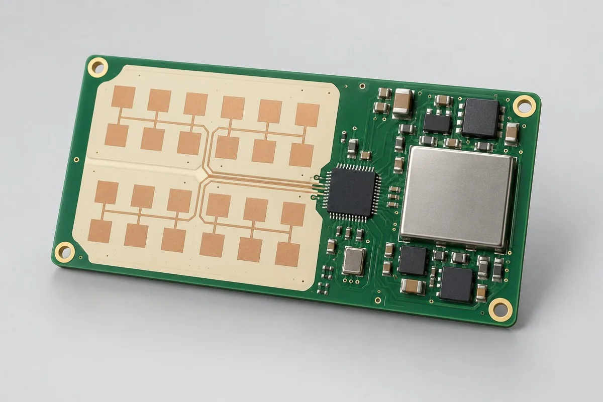
- Millimeter-Wave Presence Detection Board: Radar antenna and housing impact.
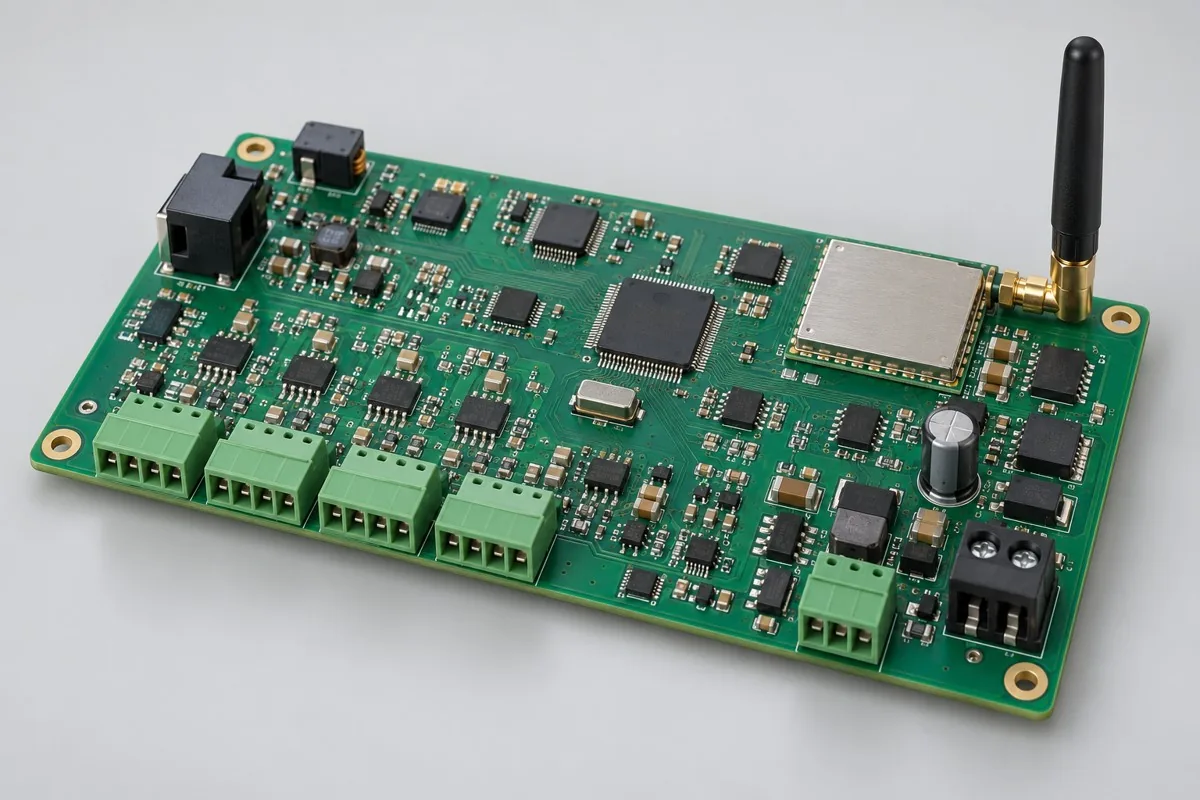
- Wireless Measurement Gateway Board: Module RF and industrial acquisition on same board.
- Multi-band wireless signal transceiver module: Engineering reference configuration; frequency bands and interfaces require project-specific definition.
When initial design files must be created
Low-power Sub-GHz wireless sensor transceiver board design: Provides access to corresponding circuits/layouts and verification plans. Channels, interfaces, or mechanics may differ from this page's engineering reference and require independent design revisions. Design-stage deliverables include source files, BOMs, layout constraints, and verification records. Assembly procurement on this page delivers actual PCB assemblies/components, programmed revisions, and product-test records against approved files.
Return to high-frequency PCB assembly configuration comparison · Component Supply and Procurement · Testing and Delivery Scope
Material and Process Reference
- Engineering reference | SMT packages and assembly methods: pads, stencils, and thermal processes: a package/assembly method index only; not evidence that the product configurations on this page are models produced by KFPCBA
- Engineering reference | Moisture-sensitive component management: MSL, floor life, and reflow conditions: a basis for moisture-sensitive component management methods only; not evidence of KFPCBA equipment, qualifications, or order scope
To request an assembly review, send an RFQ with the quantity, BOM revision, assembly files, material-supply responsibilities and required test records. Agree any design or test work separately.