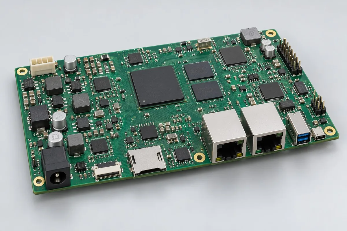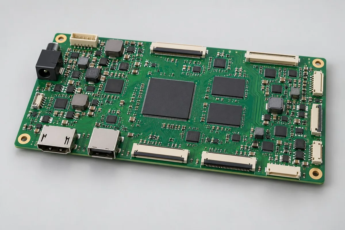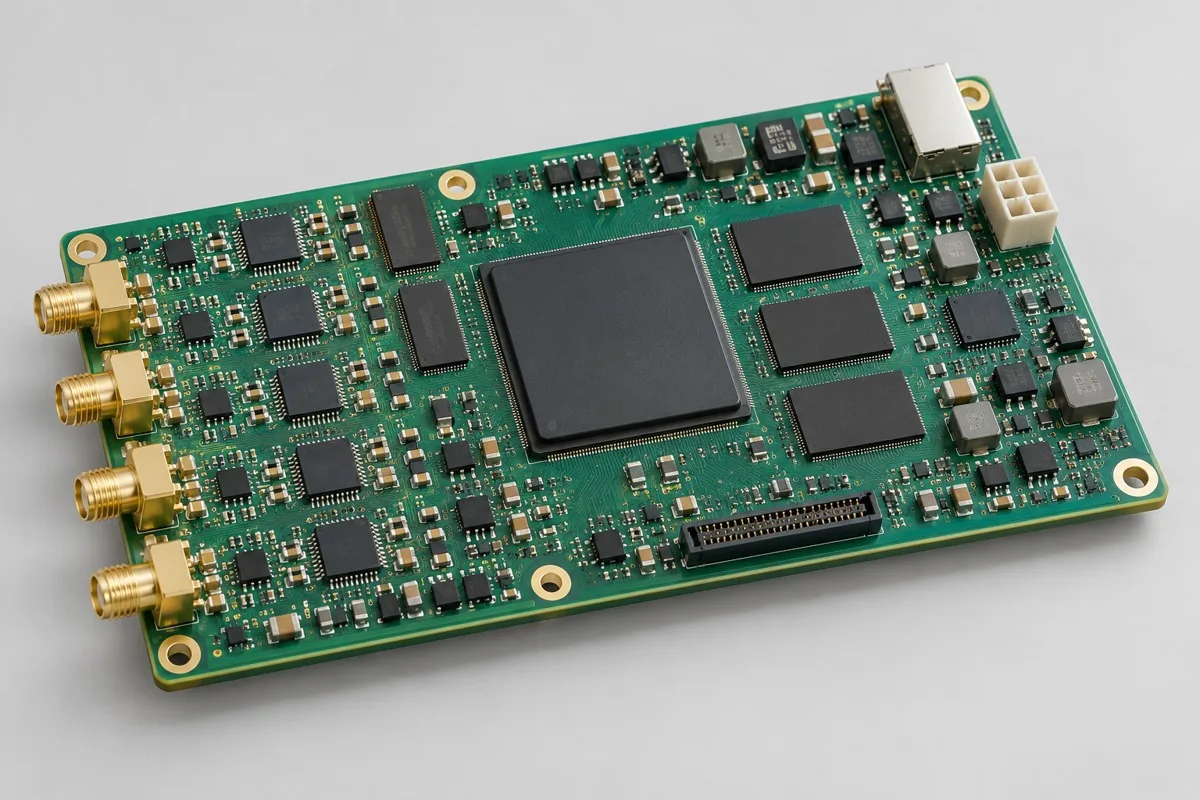
Engineering Reference Configuration
FPGA acquisition board assembly: assembly configuration and test deliverables
The following adjustable engineering configurations support material, functional, and process review; they are not stocked models or commitments to current production-line capabilities. Approved fabrication documentation and order acceptance requirements govern.
This FPGA PCB assembly engineering reference uses an 8-channel analog front end, with 4/16-channel variants requiring separate design and test review. First confirm FPGA + ADC + buffer memory, Ethernet or USB data output, synchronous trigger input, and 6/8-layer FR-4 with high-speed routing and reference-plane partitioning. Then compare double-sided SMT, BGA temperature profiling and hidden-joint verification, post-installed connectors, and acceptance costs for power sequencing, clocks, channels, memory read/write, and output links. This page separates the board + channel mapping + program checksum + test records from optional external calibration sources, trigger cables, and acquisition software, helping determine whether quotations cover the actual application. Quotation documentation reference:BOM · bare board · material supply
Reference specification and configuration options
| Options | Reference Configuration |
|---|---|
| Power and Logic Domains | 12V input; 3.3V interface logic |
| Functional Module | 8-channel analog front end, adjustable to 4/16 channels |
| Core Components/Architecture | FPGA + ADC + buffer memory |
| Interface and Channels | Ethernet or USB data output; synchronous trigger input |
| Board Layers and Material Options | 6/8-layer FR-4; high-speed routing and reference-plane partitioning |
| Component packages | BGA processor/memory, QFN ADC, surface-mount passive components |
| Assembly Route | Double-sided SMT; BGA temperature profiling and hidden-joint verification; connectors installed afterward |
| Material Supply Scope | Customer-specified FPGA/ADC; common passive components may be sourced |
| Firmware and Parameters | Separate revisions for FPGA bitstream, controller firmware, and sampling parameters |
| Test Focus | Power sequencing, clock, channels, memory read/write, and output path |
| Deliverables | Board + channel mapping + program checksum + test records |
| Configuration Limits/Options | Optional external calibration sources, trigger cables, and acquisition software |
How much does FPGA data acquisition board PCB assembly cost, and what is included?
FPGA, ADC, and buffer memory are key material-pricing items. Itemize double-sided placement, BGA joint inspection, bitstream programming, synchronous sampling, and continuous-output tests. External calibration sources, trigger cables, and acquisition software are not automatically included in board assembly unit prices. Equal channel counts can still produce different prices when test durations, buffer depths, or output requirements differ.
Quotation terms depend on the approved files, quantity, material supply, tests and delivery requirements.
Prepare a structured RFQ or use the short inquiry form.
| Cost Item | Scope for This Configuration | Billing frequency and work scope | Procurement Verification |
|---|---|---|---|
| Bare PCB and core components | FPGA + ADC + buffer memory; 6/8-layer FR-4; high-speed routing and reference-plane partitioning | Price according to actual bare-board/component purchase quantities; authorize critical components and substitutions individually | Customer-specified FPGA/ADC; common passive components may be sourced |
| Placement and secondary assembly | Double-sided SMT; BGA temperature profiling and hidden-joint verification; connectors installed afterward | Feeder/program setup per lot; assembly priced per board, joint, or process as agreed, with counting rules specified | BGA processor/memory, QFN ADC, surface-mount passive components |
| Manufacturing Preparation | Review stencils, first articles, and support tooling against the actual assembly route | New stencils/carriers may be separate one-time charges; verify panelization, revision, and condition before reuse | Reduced quantities do not automatically eliminate first-article or feeder setup |
| Test resources and execution | Power sequencing, clock, channels, memory read/write, and output path | Itemize test-method/fixture/script setup; agree execution charges per board, channel, or test duration | Separate supporting development from execution records for each board |
| Software and Parameters | Separate revisions for FPGA bitstream, controller firmware, and sampling parameters | When firmware exists, distinguish file programming/verification from software development; omit programming without a firmware revision | Customer-approved files, parameters, and readback rules determine scope |
| Delivery and Change | Board + channel mapping + program checksum + test records; optional external calibration sources, trigger cables, and acquisition software | Price accessories, retesting, and revision changes by approved work items; do not prefill fixed rates | Check BOM, tooling, programs, and acceptance revisions before reorders |
How should FPGA and MCU acquisition boards be selected?
Compare synchronous triggering, ADC reading, buffering, and continuous-transmission tasks before processor names. FPGA suits parallel timing tasks but requires maintainable bitstreams and verification conditions. If an MCU meets targets, it can reduce component and software-maintenance complexity. The 8-channel AD module emphasizes measurement range and calibration; this board emphasizes synchronization and data links under approved bitstreams.
| Comparison Metric | Current Conditions | Factors Influencing Procurement Decision |
|---|---|---|
| Manufacturing Delivery | Double-sided SMT; BGA temperature profiling and hidden-joint verification; connectors installed afterward | Produce boards/assemblies per BOM and assembly drawings; this does not establish that every system function passes |
| Functional Acceptance | Power sequencing, clock, channels, memory read/write, and output path | Compare unit prices after defining test stimuli, limits, accessories, and records; review missing test inputs first |
| Configuration Options | Ethernet or USB data output; synchronous trigger input; 6/8-layer FR-4; high-speed routing and reference-plane partitioning | Confirm circuit/program compatibility before reviewing assembly and test costs for interface, stackup, or component changes |
| Delivery Scope | Optional external calibration sources, trigger cables, and acquisition software | Complete-system accessories, application development, and project verification are not automatically included in board assembly |
Should 8-channel acquisition use USB or Ethernet?
Calculate sustained data volume from actual sample formats, then account for protocol overhead, buffering, and host reception capability. USB suits nearby host acquisition; Ethernet suits network connections. Interface names do not replace measured throughput. Align per-channel sampling requirements, simultaneously enabled channels, continuous-test duration, and allowable sample-loss conditions when comparing quotations.
- First list the required 8-channel analog front end, adjustable to 4/16 channels, distinguishing build-to-print manufacturing, configuration adjustments, and new-function development.
- Then freeze complete part numbers for FPGA + ADC + buffer memory, Ethernet or USB data output, synchronous trigger input, and 6/8-layer FR-4 with high-speed routing and reference-plane partitioning. Separate customer-supplied and sourced materials: customer-specified FPGA/ADC; common passive components may be sourced.
- Use first articles to check double-sided SMT, BGA temperature profiling and hidden-joint verification, post-installed connectors, and separately versioned FPGA bitstreams, controller firmware, and sampling parameters. If only program files are supplied, agree programming verification first; development requires separate review.
- Convert power sequencing, clocks, channels, memory read/write, and output links into acceptance items with stimuli, limits, and records; specify fixture ownership, per-board execution, and post-repair retesting.
- Finally confirm the board + channel mapping + program checksum + test records and optional external calibration sources, trigger cables, and acquisition software. Compare totals using identical quantities, accessories, and test scope, then freeze the order revision.
Applicable uses and situations requiring separate review
This page covers acquisition boards handling synchronous timing, buffering, and continuous output under approved FPGA/ADC designs. Compared with the 8-channel AD detection module, that module defines measurement range, calibration, and data budgets before processor selection. A few slow sensors do not automatically require an FPGA. Whether an MCU meets synchronization/throughput requirements depends on the specific ADC, software, and test results; architecture names alone do not establish the answer.
For a few slow sensing points where cost matters more than synchronization, compare MCU acquisition boards first. Projects without defined throughput budgets or available bitstreams should not directly use this configuration for production pricing.
Assembly Challenges for This Product
Visual inspection cannot replace inspection of joints beneath FPGAs and memory. Process verification considers package pads, fanout vias, solder volume, and board warpage together. Evaluate ADC analog regions alongside high-thermal-mass BGA placement, with first-article profiling points near both component types. After rework, rerun clock, buffer, and all-channel tests; reprogramming alone is insufficient for release.
Structural, thermal, and configuration trade-offs
More layers improve signal returns and power distribution but increase bare-board and prototype costs. Install heat sinks after reflow; include thermal-interface material thickness and clamping methods in mechanical drawings. Do not arbitrarily change FPGA speed grades to reduce temperature rise.
Configuration-specific test matrix
| node | Inspection/Functional Methods | Acceptance Record |
|---|---|---|
| Power-On/Clock | Power up with current limiting; record steady-state values and startup timing for each rail, and check the reference clock | Power curves, clock results, and program revision |
| Sampling chain | Distribute a signal from the same reference source to 8 channels; observe zero offset, amplitude, and relative channel timing | Channel records; thresholds from approved test specifications |
| Buffer/output | Read/write the buffer, then transmit continuously with packet-loss counts and trigger events | Data samples and error counts, with test duration recorded |
Defect Handling and Acceptance
Locate solder bridges or opens using hidden-joint inspection and functional symptoms. For ADC zero-offset anomalies, first distinguish soldering, reference-source, and calibration-parameter causes. Acceptance requires more than communication; retain each channel's results and links to post-rework retesting.
FPGA acquisition boards: material supply and revision management
Lock FPGA, ADC, and memory to complete ordering part numbers; handle loose or salvaged components separately from original-packaged parts. Customer-supplied critical ICs require opening, MSL, and remaining-material records. Sourced passive components also require authorized substitution rules.
Prototyping vs. Production Differences
Samples may retain jumpers, segmented power, and debug interfaces. Before production, freeze bitstreams, BOMs, and fixture contact points, converting manual oscilloscope observations into channel tests with saved results.
Delivery Configuration
Board + channel mapping + program checksum + test records. External calibration sources, trigger cables, and acquisition software are optional.
Convert this configuration into a reviewable order
For FPGA multichannel acquisition board orders, check BOM, quantity, material supply, and the conditions below. Add pick-and-place files, DNP lists, and assembly drawings for SMT. For programming, provide separately versioned FPGA bitstreams, controller firmware, and sampling parameters with files, programming rules, and verification requirements. Review costs separately for materials, double-sided SMT, BGA temperature profiling and hidden-joint verification, post-installed connectors, required stencils/feeder setup, support carriers, and test resources. Documentation changes require renewed revision approval; agree delivery milestones after material readiness and scheduling confirmation.
| Project inputs required for review | Engineering decisions | Records/delivery as agreed in the order |
|---|---|---|
| Sampling Throughput and Synchronization | Provide per-channel sampling modes, sustained output rates, trigger timing, and allowable packet loss to determine buffering, test duration, and bitstream revision. | Record each channel's data and packet-loss counts; link raw samples to board numbers and bitstream checksums. |
| Critical IC Material Supply | Freeze FPGA speed grades, ADC packages, and memory part numbers before determining assembly/programming resources. | Trace critical-component lots, MSL handling, and program revisions separately. |
FPGA data acquisition board PCB assembly FAQs
How much does FPGA data acquisition board PCB assembly cost, and what is included?
Count standard placement and QFN/BGA points separately, then add setup, subsequent installation, and inspection fees. A project-specific quotation requires review of the available files, quantity, materials, requested tests, delivery destination, taxes, shipping, and trade terms. Agree the billing unit and currency in the quotation; list bare PCBs, BOM components, and testing separately. No current unit prices are published here; request an itemized quotation for the approved scope.Review quotation inputs and scope.
How should FPGA and MCU acquisition boards be selected?
Compare synchronous triggering, ADC reading, buffering, and continuous-transmission tasks before processor names. FPGA suits parallel timing tasks but requires maintainable bitstreams and verification conditions. If an MCU meets targets, it can reduce component and software-maintenance complexity. The 8-channel AD module emphasizes measurement range and calibration; this board emphasizes synchronization and data links under approved bitstreams.
Should 8-channel acquisition use USB or Ethernet?
Calculate sustained data volume from actual sample formats, then account for protocol overhead, buffering, and host reception capability. USB suits nearby host acquisition; Ethernet suits network connections. Interface names do not replace measured throughput. Align per-channel sampling requirements, simultaneously enabled channels, continuous-test duration, and allowable sample-loss conditions when comparing quotations.
Is FPGA bitstream development included in PCB assembly charges?
Bitstream development differs from programming supplied files. Assembly quotations should separately list bitstream programming/verification, controller firmware, and sampling-parameter loading. Implementing new logic without an available bitstream is development, not a single programming operation.
Can BGA inspection replace eight-channel sampling tests?
BGA inspection addresses hidden joints, not analog-channel gain, synchronization, or buffered output. Prototype-level verification and production-release items can be agreed separately, but each channel mapping and active data link still requires results.
What dedicated test conditions are needed for small-batch FPGA acquisition boards?
First provide usable bitstreams, trigger events, and an acquisition host; define per-channel mappings, buffer read/write, and continuous-transmission records. Synchronization and throughput targets affect fixture/software setup. Before production, convert debugging observations into saved per-board results.
Can common components be sourced while the customer supplies FPGA and ADC components?
Separate critical ICs and common components under an authorized BOM. Freeze FPGA speed grades, ADC packages, and memory part numbers; provide opening and lot records with customer-supplied materials. Check passive substitutions against analog and clock applications too.
How should power-up/clock testing be included in FPGA acquisition board procurement acceptance?
The reference method uses current-limited power-up, recording steady-state values and startup timing for each rail and checking the reference clock. Records should include power curves, clock results, and program revisions. Supply test inputs, applicable configurations, and acceptance limits with the inquiry, then agree first-article verification and per-board execution scope. Price test-resource setup separately from each execution. Methods can be reviewed before limits are available, but completing an operation does not establish specification compliance.
How should sampling-chain testing be included in FPGA acquisition board procurement acceptance?
The reference method distributes a same-source signal to 8 channels, observing zero offset, amplitude, and relative timing. Keep channel records using thresholds from approved test specifications. Supply test inputs, applicable configurations, and acceptance limits with the inquiry, then agree first-article verification and per-board execution scope. Price test-resource setup separately from each execution. Methods can be reviewed before limits are available, but completing an operation does not establish specification compliance.
How should buffer/output testing be included in FPGA acquisition board procurement acceptance?
The reference method reads/writes buffers and then transmits continuously with packet-loss counts and trigger events. Records include data samples, error counts, and test duration. Supply test inputs, applicable configurations, and acceptance limits with the inquiry, then agree first-article verification and per-board execution scope. Price test-resource setup separately from each execution. Methods can be reviewed before limits are available, but completing an operation does not establish specification compliance.
What costs should be itemized when changing FPGA boards from manufacturing-test to shipping bitstreams?
First lock separate checksums for test bitstreams, controller firmware, and final sampling parameters. After manufacturing tests, itemize final-file programming, readback, and final synchronous-sampling/buffer-output verification. If final bitstreams change clocks or channel mappings, review test resources against new cases; passing with a test bitstream does not establish that the shipping configuration passes.
Is FPGA acquisition board BGA hidden-joint inspection priced per component or per board?
This page specifies BGA processors/memory, QFN ADCs, and surface-mount passive components. List actual BGA part numbers, quantities, and joint-inspection scope before agreeing charges per component, board, or inspection time. Define methods, inspection coverage, image retention, and post-rework reinspection. Power sequencing, clocks, channels, memory read/write, and output links require independent confirmation. Determine inspection dimensions, coverage, and equipment methods with actual packages; the BGA designation alone does not establish them.
How are setup charges calculated for additional small lots when customer-supplied FPGA or ADC deliveries are incomplete?
Confirm deliverable board quantities against complete FPGA speed grades, ADC packages, and the memory BOM; do not fill shortages with unauthorized substitutions. For additional lots, itemize renewed feeder setup, first articles, and bitstream/synchronous-sampling resource checks. Verify existing stencil/fixture reuse by revision and condition. Record remaining-material and replacement-loss responsibilities in the material list; do not assume the second lot has no setup charge.
What requires retesting after FPGA acquisition board repairs or repeat orders?
Select retests by change impact. Original acceptance covers power sequencing, clocks, channels, memory read/write, and output links; shipping records include the board + channel mapping + program checksum + test records. Repairs affecting power, interfaces, critical analog circuits, or software revisions require related tests, beyond repaired joints. Repeat orders must align with original BOMs, parameters, and test resources. Agree retest charges by approved items and actual quantities; do not assume free service or fixed turnaround.
How should FPGA acquisition board pricing for 6 and 8 layers be compared?
6/8-layer FR-4 are reference options, not two verified stocked models. Align stackup, reference planes, high-speed routing constraints, and approved Gerber files before comparing bare-board and assembly pricing. Layer-count changes require layout and signal-condition review; an 8-layer fabrication price does not imply higher sampling performance.
How are FPGA acquisition board fixture charges separated from per-board test charges?
Trigger sources, eight-channel signal distribution, acquisition hosts, and buffer/output scripts are test resources; setup or modification can be itemized. Per-board power sequencing, clocks, channels, and continuous transmission are priced by approved execution items. Specify fixture ownership, reuse revisions, customer-provided calibration sources, and result retention to avoid repeatedly charging one-time setup as a fixed per-board cost.
Why does adding FPGA acquisition channels cost more than the ADC price difference?
Changing this page's 8-channel front end to 4/16 channels is an engineering option. Channel changes affect the front end, ADC reading, FPGA bitstream, buffering, sustained host reception, test connections, and channel records. Approve new BOMs and programs before calculating revision, assembly, and per-channel testing costs. Adding components alone does not establish usable new channels.
Compare Other Products in This Category
- BGA communication gateway motherboard: Network processors, memory, and interface connectivity.
- 8-channel analog acquisition module: Prioritize measurement range and per-channel calibration; select processors by data budgets.
Return to BGA PCB assembly configuration comparison · Component Supply and Procurement · Testing and Delivery Scope
Material and Process Reference
- Engineering reference | BGA assembly methods: pad definitions, warpage, and hidden solder joints: methods for BGA pads, temperature profiling, and hidden solder joint inspection. Use current manufacturer documents for each component; do not transfer example limits
- Engineering reference | Moisture-sensitive component management: MSL, floor life, and reflow conditions: a basis for moisture-sensitive component management methods only; not evidence of KFPCBA equipment, qualifications, or order scope
To request an assembly review, send an RFQ with the quantity, BOM revision, assembly files, material-supply responsibilities and required test records. Agree any design or test work separately.