Why do high-frequency PCB assembly quotes require more than solder joint counts?
Quotes should separately itemize RF component and connector procurement, shield and antenna assembly, calibration setups and fixtures, and link, port, or sensing functional tests. Separate initial order setup costs from recurring batch and per-board costs. For the same quantity, also align revisions, delivery configuration, and tax and shipping terms to determine whether price differences reflect configuration or excluded work.
Quotation terms depend on the approved files, quantity, material supply, tests and delivery requirements.
Prepare a structured RFQ or use the short inquiry form.
How does RF assembly inspection differ from complete antenna product testing?
Millimeter-wave sensing, RF transceiver, and wireless gateway frequencies serve different purposes. Placement inspection cannot replace RF testing. Board-level port testing and application verification with antennas and enclosures are also different cost items.
How should test configurations be selected for millimeter-wave sensing and RF transceiver boards?
First select actual frequency bands, bandwidth, and ports, then determine antennas, shielding, and test reference planes. A module starting up does not establish link or sensing performance inside an enclosure.
High-frequency PCB assembly: order scope and acceptance
High-frequency PCB assembly requires joint review of RF component assembly, matching networks, shield/antenna construction, and link testing. Radar, transceiver boards, and wireless gateways have different acceptance requirements. Fabricator impedance parameters cannot replace complete board RF results.
Sensing boards: antenna/enclosure/algorithm; RF interfaces: matching/calibration plane; gateways: acquisition/wireless concurrency; mobile signal transceivers: band paths/gain combinations.
Differences in assembly and test paths
RF path checks cannot rely on appearance alone. Establish checkpoints for modules, connectors, and shield installation, and separately accept sensing scenarios, link curves, network recovery, and band switching.
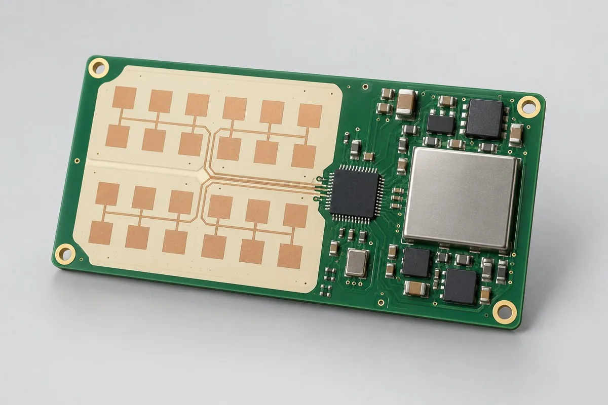
Millimeter-Wave Presence Detection Board
SMT → hidden solder joint verification → RF inspection → parameter programming. Isolate soldering defects separately from antenna/algorithm issues. For startup failure, check power and package connections first. For missed detection in specific directions, check mechanical construction, antennas, and parameters. The acceptance matrix must record targets, placement, and environment.
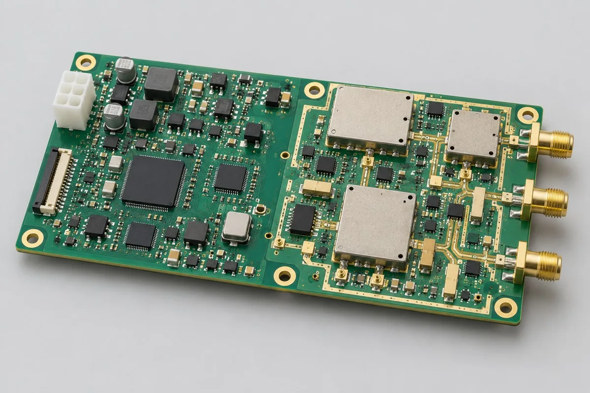
RF Transceiver Interface Board
RF SMT → connector soldering → pre-shield inspection → link testing. Incorrect matching capacitors, shield shorts, or poor coaxial socket soldering may appear only as link attenuation. Use approved curve limits and measurement conditions for acceptance; instrument readings do not represent performance under every installation condition.
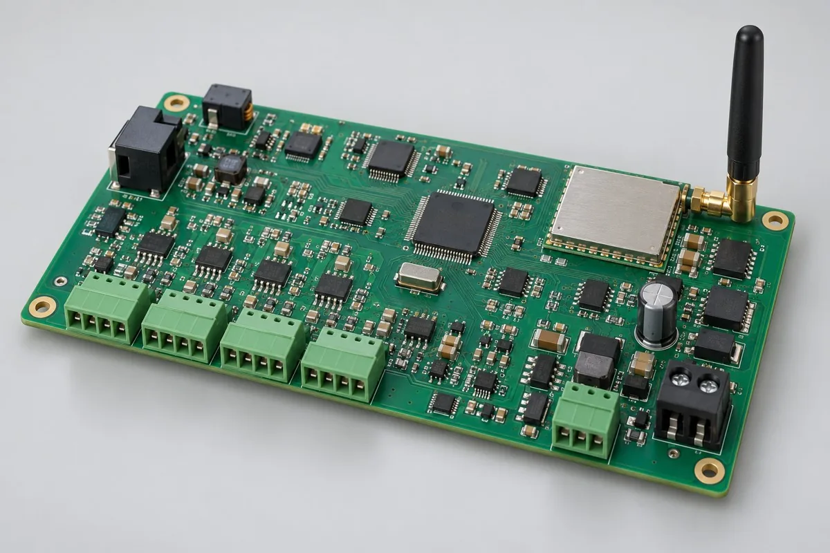
Wireless Measurement Gateway Board
Double-sided SMT → secondary terminal soldering → antenna connection → calibration/networking. Channel drift, module resets, and packet loss correspond to analog, power, and protocol layers respectively. Retain data-handling results during offline periods. Network connection alone does not cover sensor channels.
Multi-band wireless signal transceiver module
SMT → connectors/shielding → firmware → per-band link testing. Handle incorrect filters, wrong switching paths, poor connector soldering, and mismatched calibration tables separately. Define bands, directions, and measurement reference planes for acceptance. Signal reception alone does not establish consistent module-wide performance.
RF test support included in quote
Define bands/ports, antennas or attenuators, reference planes, and parameter revisions. Radar needs scenarios, transceiver boards need ports, and gateways need data paths; normal power-on cannot provide a common release criterion. Bands and functions: enabled bands, transmit/receive directions, and link budget. Component frequency bands do not establish complete board performance. Assembly files: specified RF part numbers, locations, shielding, and antenna keepouts, with later-installed mechanical parts included in revision control.
Component supply, quantity and delivery
Include onboard antennas, external antennas, shields, and enclosures in the controlled configuration. Module certification does not automatically certify the complete product.
For the order, align Gerber /BOM pick-and-place files/DNP and assembly drawings, quantity, customer-supplied/procured material lists, and firmware verification. Delivery records include band tables, firmware/calibration, and link or scenario results, covering only approved test combinations. Confirm fees separately for stencil/carrier/fixture preparation, process operations, programming/calibration, and the supporting tests on this page. Agree on replenishment/attrition, excess materials, and change-related inventory first, then list delivery milestones after material readiness and scheduling are confirmed. Perform relevant regression testing for component/interface/mechanical/firmware changes, and record pilot issues separately from production release.
Material and Process Reference
High-frequency PCB assembly pricing and selection FAQ
Why do high-frequency PCB assembly quotes require more than solder joint counts?
For standard placement, first calculate board quantity × billable points per board × price per point + setup fee. A project-specific quotation requires review of the available files, quantity, materials, requested tests, delivery destination, taxes, shipping, and trade terms. This is a placement-only reference; bare PCBs, materials, and testing are charged separately. Any formula on this page organizes cost inputs; it is not a quoted rate.View cost items, calculation conditions, and sources.
How should I compare high-frequency PCB assembly manufacturers' quotes?
Clarify whether measurements are taken at bare board ports, on an antenna-equipped assembly, or inside the enclosure. List connectors, shield assembly, and calibration fixtures. Accepted component placement alone cannot establish RF performance.
What needs confirmation before and after RF shield installation?
Before installation, check accessible solder joints and matching components. After installation, check specified ports or links. Mechanical and grounding changes may affect results, so list inspection checkpoints in the quote rather than testing only once on an unobstructed board.
Can module-based and radar BGA designs be compared at the same SMT price?
Modules and chips integrated on the same board differ in components, assembly, and RF tuning. Fix bands, power, and enclosure first, then separate procurement, hidden solder joint inspection, and scenario testing work.
What costs can customer-supplied RF test fixtures save?
Check connectors, reference planes, calibration status, and revisions; this may reduce new fixture preparation. Per-board connection, measurement, and recording remain execution work. Having a fixture onsite does not mean port results pass.
Does changing the antenna without changing the PCB require a new test review?
Antennas and enclosures belong to the verified combination. Installation and matching changes require link or sensing checks. Assess firmware changes separately; unchanged PCB artwork does not waive retesting.
Quote for high-frequency PCBA assembly: describe the application, existing configuration, and expected quantity so we can discuss assembly inclusions and selection requirements.