PCB FABRICATION · ENGINEERING EXAMPLE
BMS PCB Engineering Example for Accurate Sensing
Engineering Application Example
Review a BMS PCB by separating sensitive measurement paths, balancing heat and power-current routing, with a traceable error budget and test plan.
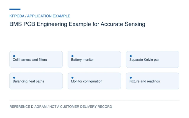
Illustrative engineering application example, not a KFPCBA customer delivery or measured production record. The configurations and calculations below are hypothetical design-review inputs. Project acceptance requires approved drawings and named engineering review.
Protect the measurement path before choosing the stackup
A battery-management PCB combines measurements that may be small with conductors and switching circuits that can create much larger disturbances. The first decision is how cell-voltage inputs, current sensing, temperature channels, balancing circuits and communication paths will coexist. More copper or more layers cannot correct a sense connection taken from the wrong physical point.
This board-level example does not define a battery pack, protection architecture or vehicle qualification. A six-layer through-hole construction may be explored during layout, but the application name does not establish that it is necessary or sufficient.
Write a measurement and operating-state brief
List the selected monitor IC, cell arrangement, harness pinout and measurement references. State the intended current-sensing method, shunt connection, temperature-sensor locations and balancing strategy. Identify which circuits remain powered during sleep and how communication and diagnostic access are provided.
Separate the accuracy target into device error, sensing-component tolerance, connection resistance, temperature effects and calibration assumptions. The system engineer should identify applicable isolation and fault requirements. Those requirements must be translated into drawings and test methods; they cannot be inferred from a laminate name or a generic BMS diagram.
Treat Kelvin pickup as a physical connection
For its BQ76952 implementation, TI emphasizes Kelvin connections at the sense resistor and close placement of the input-filter components at the monitor. This supports reviewing the complete pickup and filter path, rather than only checking schematic net names. Component values and pin treatment must follow the selected monitor's documentation.
In the proposed board review, trace both sense leads back to the intended shunt terminals. Check whether connector current, copper necks or an unintended shared segment sits inside the measurement path. Put balancing resistors and other heat sources on the placement overlay, because a temperature gradient can change the conditions under which the measurement is evaluated.
A hypothetical shunt-error calculation
Assume a 2 mΩ shunt carrying 20 A. Its ideal voltage is V = I × R = 20 × 0.002 = 0.040 V, or 40 mV. Dissipation is P = I²R = 20² × 0.002 = 0.8 W. These assumed values are an error-budget exercise, not a component selection or an operating rating.
If an unintended 0.5 mΩ current-carrying connection is included between the pickup points, it adds 20 × 0.0005 = 10 mV. That is 25% of the intended 40 mV signal. The example shows why the geometry of the connection can dominate the result even when the nominal shunt value is correct. Actual shunt power capability, thermal behavior and monitor limits require their own verification.
Make fabrication choices follow the error and heat map
Propose layer assignments after locating the monitor, connectors, shunt and balancing components. A reference plane may help organize the layout, but its return-current routes and connectivity still need review. Define finished copper and any reinforced current paths by region and layer rather than copying a copper-weight shorthand.
Use test access that does not disturb the intended sensing path. If calibration is planned, identify the measurement points, reference instrument and configuration data. The fabrication review should also cover drill and plating definitions, cleanliness requirements, board dimensions and the conditions for material substitutions.
Build a verification matrix around error mechanisms
| Risk | Review or test | Retained record |
|---|---|---|
| Shared resistance in current sensing | Pickup-point inspection and reference comparison | Connection drawing, readings and uncertainty |
| Cell-input mismatch | Controlled cell-simulator conditions across channels | Input values, channel mapping and monitor settings |
| Balancing affects measurements | Compare balancing states under defined conditions | Temperature map and voltage deviations |
| Assembly or harness changes a reading | Compare approved harness and fixture configurations | Part revisions, pinout and repeat measurements |
Use a qualified laboratory and an approved plan for battery-system and fault testing. The table defines evidence categories; it does not supply test energy, protection thresholds or pack-level acceptance criteria.
Deliver settings with the hardware records
A useful package includes fabrication and assembly files, the sensing schematic, monitor configuration, channel map, shunt specification and harness drawing. Add calibration data where applicable, firmware identifiers, fixture details and the results of agreed inspections. Label untested protection or communication functions explicitly so they are not assumed to be covered by a board test.
To begin an assessment, describe the monitor, cell arrangement and design stage. Use the quotation request to provide available files and ask for the fabrication, assembly and test scope to be defined separately.
BMS layout questions
Can calibration remove a poor Kelvin connection?
A fixed correction may not remain valid as current distribution or temperature changes. Correct the connection geometry first, then evaluate any remaining calibration need under the intended conditions.
Should balancing be disabled during every measurement?
That depends on the selected monitor and measurement strategy. Define the timing and compare the relevant states; do not import a balancing sequence from a different IC.
Does a bare-board electrical test validate BMS protection?
No. It checks the agreed board connectivity. Monitor settings, sensing accuracy, firmware behavior and pack protection require additional tests with their own criteria and accountable owners.
Source material and applicable scope
- Texas Instruments — BQ76952 Data Sheet, SLUSE13B. Section 18 supports the device-specific discussion of Kelvin sensing and monitor-side filter placement; it is not a generic pack safety approval. These sources do not establish KFPCBA delivery or capability.