
DFM · Bare board fabrication
Check materials, stackup, copper weight, trace width/spacing, hole types, and surface finish. Deliver an approved stackup, drill table, process drawings, and CAM issue list.
DFMA translates design requirements into specific manufacturing actions: first check PCB stackup, traces, and holes, then packages, panelization and soldering conditions, and finally test points, programs, and fixtures. The review delivers a change list identifying layers, nets, reference designators, and dimensions, rather than a manufacturability conclusion without actionable results.
Consult DFMA review →
Check materials, stackup, copper weight, trace width/spacing, hole types, and surface finish. Deliver an approved stackup, drill table, process drawings, and CAM issue list.
Check BOM footprints, pick-and-place side designations, tooling rails, support, stencil, and thermal processes. Deliver panelization recommendations, assembly issues, and a first article plan.
Check test points, accessible space, electrical nets, programming interfaces, and functional cases. Deliver a coverage matrix, fixture/program requirements, and decision criteria.
| Inspection Objects | Specific Inspections | Recommendations or Delivery |
|---|---|---|
| Materials and Stackup | Material grade, layer-by-layer copper weight, dielectric thickness, lamination structure, total board thickness and tolerance; reference layers for high-speed signals | Approved stackup; dielectric, thermal, and reliability effects of substitute materials |
| Routing and Solder Mask | Minimum trace width/spacing relative to copper weight; solder mask dams, openings, silkscreen over pads, and copper-to-edge clearance | Coordinate/net location drawings; compensation, rerouting, or solder mask opening recommendations |
| Holes and Connections | Through-hole/blind via/buried via layer spans, drilled versus finished hole definitions, annular rings, aspect ratio, hole filling, and backdrill stubs | Separate PTH/NPTH and layer-spanning hole files; drill table and special process drawings |
| Outline and Surface Finish | V-scores/routed slots, panelization, mounting holes, gold fingers, contact areas, and surface finish compatibility | Confirm outline and assembly tolerances to prevent enclosure fit problems after fabricator shape changes |
| Inspection Objects | Specific Inspections | Recommendations or Delivery |
|---|---|---|
| BOM and coordinates | Full manufacturer part numbers, package dimensions, reference designators, side designations, rotation definitions, DNP, and substitution approvals | Cross-check Gerber/BOM/pick-and-place files/assembly drawings; resolve footprint and polarity conflicts first |
| Panelization and Clamping | Tooling rails, global/local fiducials, thin-board support, protruding bottom components, and component-to-depanelization-line clearance | Panelization and support/carrier drawings; assess depanelization stress and connector overhang |
| Stencil and Solder Paste | Aperture area ratio, thickness, QFN thermal pad windowing, and conflicting solder volume needs of fine-pitch and large pads | Review stencil regions or steps; verify printing and inspect solder paste volume |
| Reflow and Mixed Assembly | Solder system, component MSL/temperature limits, copper weight, double-sided sequence, and subsequent wave/secondary soldering thermal exposure | Set profiles from measured solder joint temperatures; separately confirm heat-sensitive components and mixed-technology assembly routes |
| Inspection Methods | Design/Customer Input | Test Boundaries and Output |
|---|---|---|
| AOI /Appearance | Visible solder joints, polarity markings, reference photos, and component obstruction | Identify visible defects; cannot independently assess BGA underside solder joints or circuit function |
| X-ray | Hidden BGA/QFN solder joints, critical areas, void criteria, and sampling rules | Inspect internal morphology; an image alone does not establish an electrical or functional test pass |
| ICT /Probing | Netlist, test points, accessible sides, component isolation conditions, and probe clearance | Design accessibility and coverage matrix; separately confirm fixtures and programs |
| FCT /Programming | Interface wiring, power/loads, firmware checksums, test steps, and upper/lower limits | Output SN/revision/raw measurements/pass-fail decisions; explicitly list uncovered items |
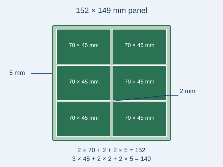
Assume 2 columns along the 70 mm dimension, 3 rows along the 45 mm dimension, 2 mm clearance between PCBs, and a 5 mm panel border on all four sides. The panel is 152 × 149 mm: width = 2×70+2+2×5; height = 3×45+2×2+2×5.
Then check fiducial locations, V-scores or mouse bites, component clearance from depanelization lines, connector protrusions, and bottom-side support. Suitable individual board dimensions do not mean the panel can travel through the entire production line.
Assume a rectangular aperture of 0.25 × 0.30 mm and stencil thickness of 0.12 mm. The area ratio is aperture area ÷ sidewall area, or 0.075÷[2×(0.25+0.30)×0.12]≈0.568.
Reducing thickness to 0.10 mm gives approximately 0.682, but also reduces solder volume on large pads. Consider apertures, stencil manufacturing processes, and solder volume needs of different components together; do not simply make the entire stencil thinner.
Page 11 of TI SLUA271C discusses apertures with area ratios below 0.66 and electroformed nickel stencils. This is a reference for the document's QFN/SON printing methods, not a universal acceptance guarantee. Confirm with the stencil supplier, then verify through printing trials.
| Issue Localization | Risks and Optional Modifications | Closure Basis |
|---|---|---|
| U12: open vias beneath the QFN thermal pad | Potential solder wicking; evaluate via treatment, location, and stencil windowing while balancing heat dissipation, cost, and solder volume | Update pad/hole process drawings, inspect pilot-run solder joints, and verify temperature rise |
| J3: Connector extending to process edge | Clamping, soldering, or depanelization force conflicts; adjust panelization/connector sequence or design a carrier | Customer-approved panelization, physical trial assembly, and depanelization inspection |
| TP7: Test points obscured by structural parts | Inaccessible to probes at the finished stage; move test points, change the test sequence, or expose a test interface | Verify fixture contact and update the coverage matrix and test steps |
Align revisions of Gerber files, drills, stackup, schematics/netlist, BOM, pick-and-place files, assembly/mechanical drawings, and test specifications; list missing items.
Locate bare PCB, assembly, and test issues separately, then check cross-effects of changes on materials, procurement, assembly, and cost.
Provide change options, impacts, responsible persons, and responses for each issue. Do not substitute critical materials or change the stackup without approval.
Deliver the issue list, approved files, open exceptions, and verification plan. Move to production after first article/pilot-run records are confirmed.
The final package includes an illustrated issue list, approved stackup and drill table, panelization/stencil recommendations, assembly notes, test coverage matrix, customer responses, and one controlled production revision. Define in the commissioned scope whether design changes, simulation, fixture fabrication, and program development are included.
Submit existing files directly for joint review. For projects still in design, first check commissioned inputs and manufacturing constraints.
Engineering reference | Packaging PCB fabrication files: units, layer order, and engineering notes: methods for PCB fabrication, hole layer spans, and file semantics.
Engineering reference | QFN and SON assembly: thermal pads, printing, and solder joint verification: QFN/SON pad, stencil, and measured thermal process methods; not company capabilities.
Engineering reference | PCB assembly panelization and tooling rails: alignment, support, and depanelization: process input references from other manufacturers; dimensional conditions do not apply to every factory.
| Work area | Inputs or responsibility | Expected output |
|---|---|---|
| Finding | Affected reference, layer, hole or operation | State the actual manufacturing conflict |
| Proposed disposition | Design change, process change or accepted exception | Name the decision owner |
| Release evidence | Changed file and revision or approved exception | Check the response appears in the released data |
| Verification | Review or trial needed after the change | Record closure rather than only an email reply |
Use the controlled fabrication package to prepare the discussion. Unknown inputs should be listed as open questions; they do not authorize substitutions, omitted tests or unrecorded design changes.

Tell us the product use and which files are available. We can define the next engineering step even when the data package is not complete.