Controlled-impedance PCBs: matching net targets to test coupons
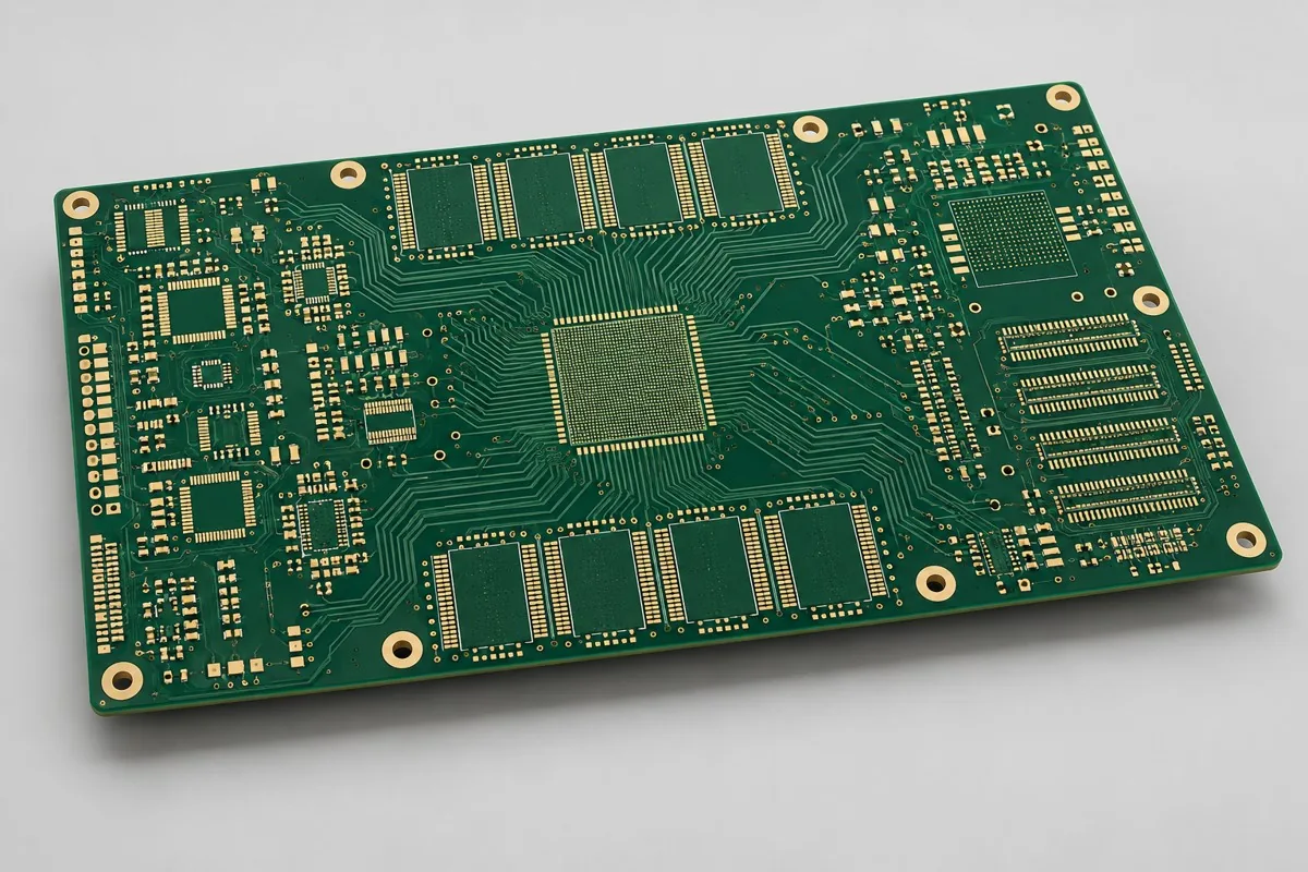
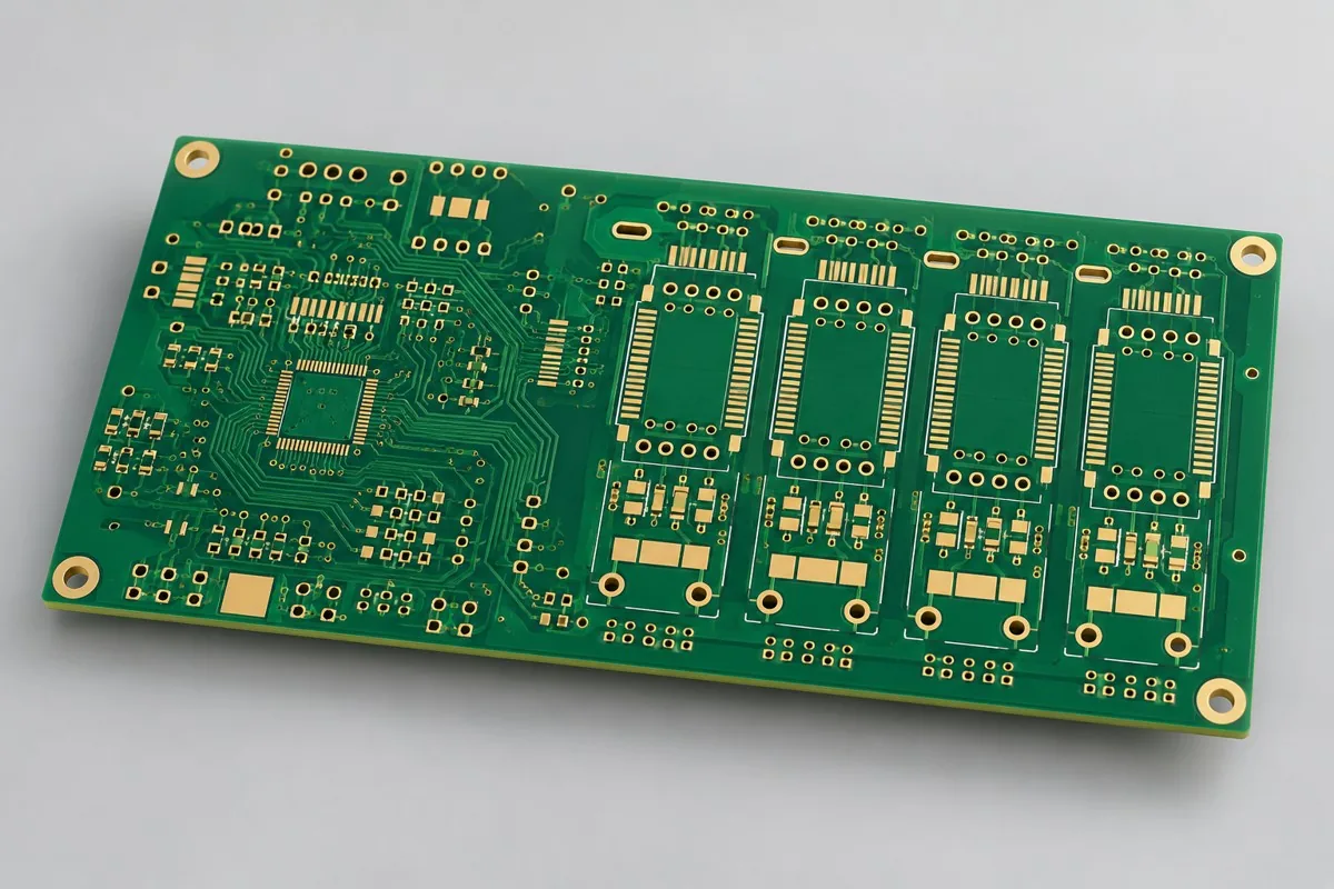
For controlled-impedance PCB fabrication, list targets, layer numbers, reference planes, tolerances, and coupon locations for each net. Confirm single-ended or differential geometry separately for USB, MDI, and DDR, with quotations based on solving the actual Layer Stackup; deliver TDR results for the corresponding layers and manufacturing revision, while interface functions and timing require separate prototype verification.
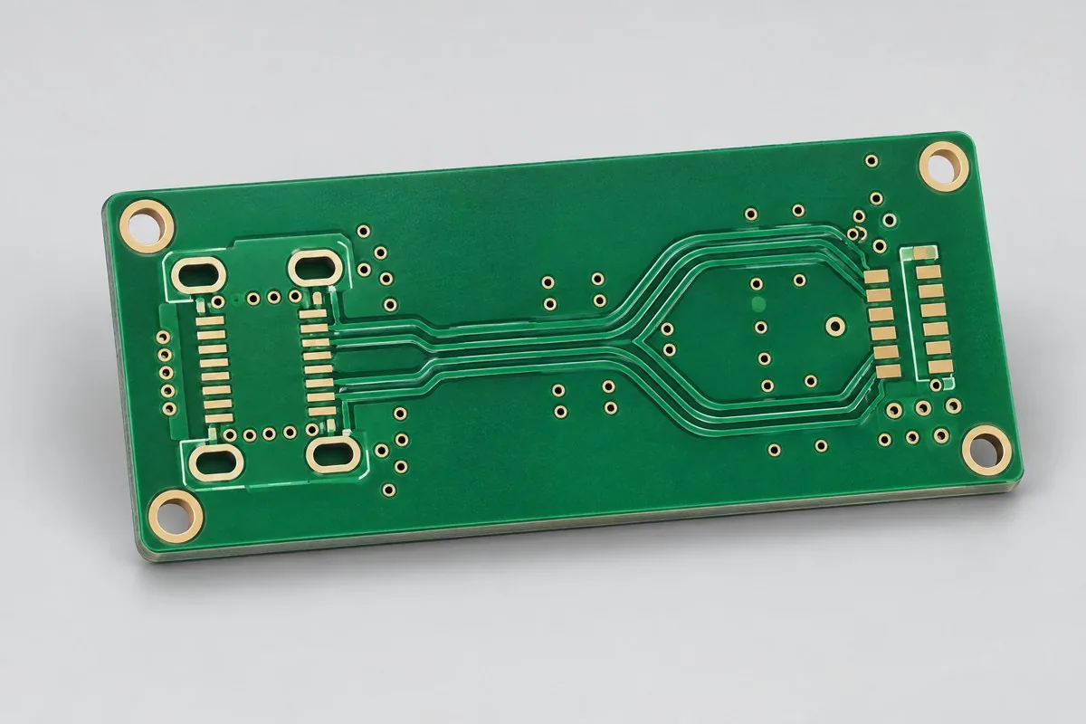
Coupon must correspond to real network
The order table lists targets, layer numbers, reference layers, trace widths/spacings, and measurement methods by net. DDR single-ended, USB differential, and acquisition differential nets cannot share one vague impedance-pass conclusion.
Impedance-controlled orders: net tables and same-layer test coupons
After selecting a product in this category, submit target nets, layer numbers, reference planes, trace widths/spacings, tolerances, and test coupons. Match each change to the Engineering Reference Configuration, using the same revision for fabrication drawings, inspection locations, and material approvals; define specialized verification and report scope before quotation.
Back to all PCB products · Manufacturing file knowledge
Material and Process Reference
Consult selected PCB configuration
How does impedance testing differ from standard PCB electrical testing?
Standard electrical testing checks net continuity; impedance testing targets specified transmission structures. USB, Ethernet, and DDR differ in targets, reference layers, and connections. Adding impedance requirements does not automatically include all interface-performance tests.
How should impedance nets and reference layers be selected for USB, Ethernet, and DDR?
Determine target nets from interface specifications and circuit requirements first, then match stackup, trace width, spacing, and reference planes. Do not directly copy another board's trace width into an order with different materials or dielectric thickness.
Controlled-impedance PCB pricing and selection FAQ
Do controlled-impedance PCB quotes include testing? How do they differ from standard boards
A project-specific quotation requires review of the available files, quantity, materials, requested tests, delivery destination, taxes, shipping, and trade terms. Add specified materials, processes, and inspections not yet included to the total cost. Standard board references do not cover every configuration of this product. Any formula on this page organizes cost inputs; it is not a quoted rate.View cost items, calculation conditions, and sources.
How should I compare quotations from controlled-impedance PCB manufacturers?
Specify target nets, tolerances, test coupons, and reports, then compare them with the manufacturer's stackup. Standard electrical testing and TDR quotes cover different tasks; complete interface verification is not included in controlled-impedance board prices by default.
How should TDR coupon charges and standard electrical-testing charges be separated?
Electrical testing checks net opens and shorts; TDR checks transmission structures for approved layer pairs. List coupon drawings, quantities, methods, and reports, with clear pricing objects for each; the tests are not interchangeable.
Can trace widths be copied to a new board manufacturer if impedance targets are unchanged?
Check the new stackup's actual dielectrics, copper weight, and fabrication compensation before calculating geometry. Equal nominal board thickness does not establish direct trace-width reuse.
Which main-board information should an impedance report reference?
Match net groups, signal/reference layers, coupon identifiers, and revisions, retaining measurement methods and acceptance criteria. An unidentified value cannot establish which structure it represents.
Can a passing impedance coupon replace USB or DDR functional testing?
Coupons verify manufacturing structures, while interfaces also include connectors, vias, components, and firmware. Verify enumeration, training, and continuous data separately with prototype test cases; a passing coupon does not establish complete-link performance.
Consult impedance PCB quotation: describe the application, existing configuration, and expected quantity so we can discuss bare-board fabrication requirements, inspection, and delivery conditions.
Do controlled-impedance PCB quotes include testing? How do they differ from standard boards
Quotes should separately account for the controlled stackup and dielectric/copper thickness, target-net artwork compensation, test coupons and TDR, reports, and agreed inspections. List initial-order setup charges separately from per-batch and per-board charges; for equal quantities, also align revisions, delivery configurations, and tax and freight terms to identify whether price differences reflect configurations or excluded work.
Quotation terms depend on the approved files, quantity, material supply, tests and delivery requirements.
Prepare a structured RFQ or use the short inquiry form.