Company Address
201, Factory 6, Longhui Industrial Park, Fuqiao 3rd District, Xinhe Community, Fuhai Street, Baoan District, Shenzhen, Guangdong, China

Multilayer PCB

Define multilayer PCB construction through layer order, planes, copper balance and via spans. Align stackup, impedance and electrical-test requirements.

Multilayer PCB fabrication: layer-sequence roles and via-structure selection

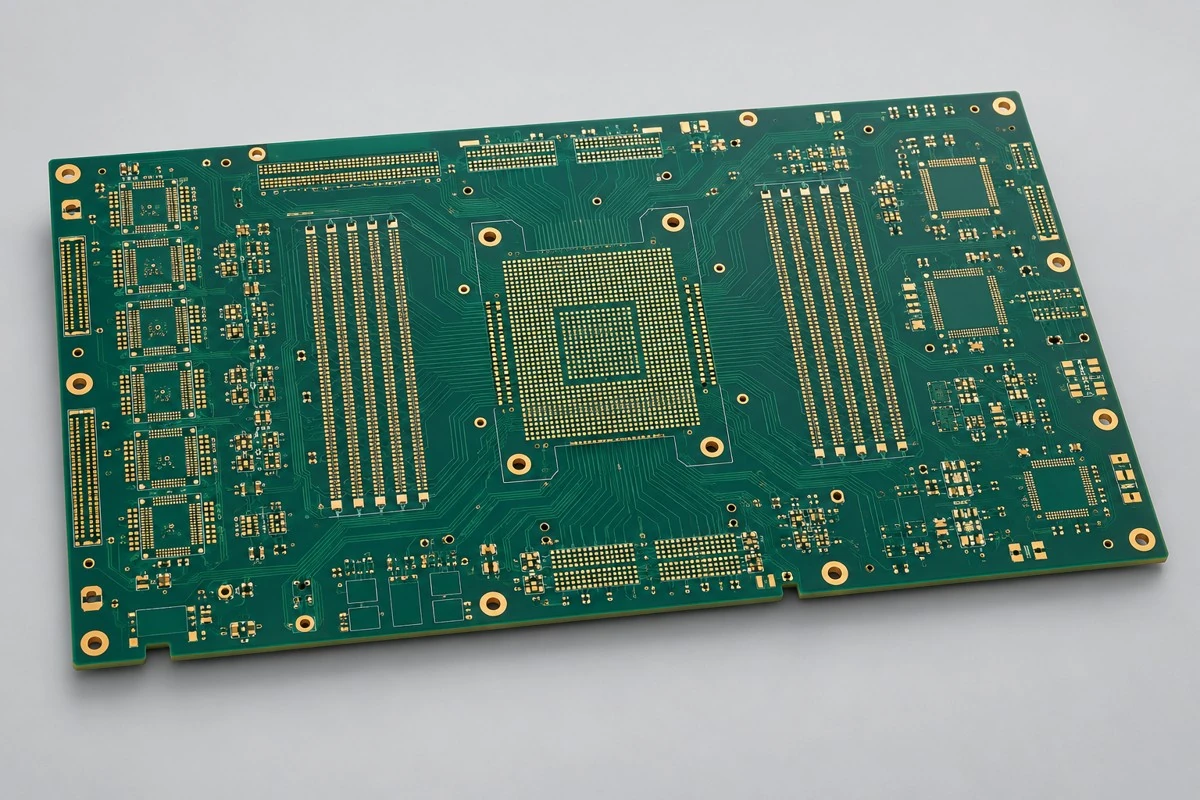
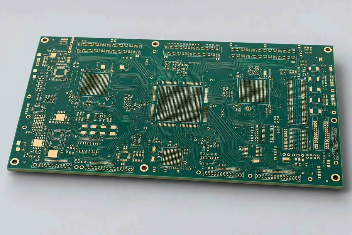
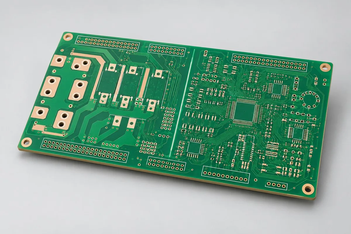
Multilayer PCB procurement requires layer-by-layer signal/power roles, copper density, and via-group drawings. Six-layer control, sixteen-layer communication, and twelve-layer backdrilled boards address power distribution, density, and transition loss respectively; deliver approved Layer Stackup and hole-wall copper records, with backdrill stub and high-speed testing scope agreed separately by board type.

Historical multilayer products: compare by application and structure

Historical ProductsOriginal specification summarySelection Focus
Press-fit hole PCB16 layers; TU-872; press-fit holes, BGA, controlled-impedance tracesPress-fit connector mating on communication boards
Semiconductor testing PCB16 layers; TU-768; press-fit holesBoard-level interconnect for semiconductor test equipment
Bonding PCBFR4; 4L/1.6mm; ENIGHistorical Bonding configuration for an embedded control board
Ten-layer 7.8 mm ultra-thick PCBHigh-layer-count board; FR4 S1000-2M; 10L/7.8mmHole structure review for ultra-thick historical special boards
Eighteen-layer communications PCBFR4 S1000-2M; 18L/3.0mm; ENIGLayer stack-up and via array for eighteen-layer communication boards

Press-fit hole PCB → Semiconductor Testing PCB → Bonding PCB → 10-layer 7.8mm extra-thick PCB → 18 Layer Communication PCB →

Layer Count, Reference Plane, and Via Structure

Six-layer control boards prioritize power and signal return paths; twelve-layer high-speed boards require material and residual-via-stub review; sixteen- or eighteen-layer interconnect boards determine layer sequence from net density, reference planes, and via groups. More layers do not automatically improve link loss, and thick boards cannot directly reuse thin-board hole diameters and hole-wall copper conditions.

Six-layer PCB stack-up review structure example

Multi-Layer Manufacturing From Lamination to Inspection

ProcessManufacturing Drawings Need ConfirmationInspection and recording
Core board graphics and inter-layer laminationMaterials, copper weight, layer functions, copper distribution, and dielectricInner-layer artwork inspection, approved stackup, and post-lamination thickness
Mechanical drilling/blind and buried holesHole pair, hole diameter definition, and lamination countHole positions, representative via-group microsections, and structural inspection
Copper plating and electroplatingHole copper, surface copper, and via fill/copper cap areasPlating and hole structure inspection per order agreement
Solder mask, silkscreen, and formWindow openings, characters, board outline, and special edgesDimension, appearance, board edge, and marking inspection
Electrical and Factory Acceptance TestingNetwork version, impedance coupon, and acceptance standardsElectrical testing, specified impedance, and agreed report

View PCB panel fabrication site → View corresponding equipment →

Material and Process Reference

Consult selected PCB configuration

How should eight-, twelve-, and sixteen-layer PCBs be compared?

Inverter control, communication switching, and high-speed interfaces need different reference layers and via connections. Added layers provide routing and reference planes but also add manufacturing work; design suitability cannot be judged solely by the price of each additional two layers.

How should power reference layers be allocated for high-speed interface and inverter control boards?

Allocate signals, power, and reference planes first, then evaluate interlayer vias and mechanical dimensions. Compare eight-, twelve-, and sixteen-layer boards against specific net density and verification requirements.

Multilayer PCB pricing and selection FAQ

How are multilayer PCBs quoted? Are additional layers worth the cost

A project-specific quotation requires review of the available files, quantity, materials, requested tests, delivery destination, taxes, shipping, and trade terms. Add specified materials, processes, and inspections not yet included to the total cost. Standard board references do not cover every configuration of this product. Any formula on this page organizes cost inputs; it is not a quoted rate.View cost items, calculation conditions, and sources.

How should I compare quotations from multilayer PCB manufacturers?

Check layer-by-layer materials, copper weight, holes, and stub requirements before reviewing reports. Added layers must serve defined net or reference-plane purposes; boards with different functions cannot be compared only by an added-two-layer price.

Can twelve- and sixteen-layer quotations be converted using a price per additional two layers?

Materials, via spans, copper distribution, and specified inspections also change. Compare each approved stackup item by item; layer-count difference is not the entire process difference.

Should residual via-stub requirements be included in a multilayer PCB inquiry?

If critical nets constrain stubs, provide actual layer pairs and permitted processing scope. Manufacturing must respond with processes and inspections; these are not included by default under the multilayer label.

Does changing only power-layer copper weight affect other costs?

Lamination, etching, holes, and thermal/impedance conditions require review. Separate material price differences from engineering changes and related retesting; copper weight is not merely a procurement variable.

Can a repeat order with the same layer count but a new stackup reuse original verification?

Signal-reference relationships and via connections may change; approve the new structure and link corresponding inspections. Old results support the old revision; handle repeat quantities separately from structural changes.

Consult multi-layer PCB quotation: describe the application, existing configuration, and expected quantity so we can discuss bare-board fabrication requirements, inspection, and delivery conditions.

Multi-layer quotation not just by layer count

Submit layer-by-layer signal/power uses, critical links, and via spans. List inspection requirements separately for thick-board hole-wall copper, sixteen-layer return paths, and backdrill residual stubs; review equal-layer-count boards with different via structures independently.

Multi-layer quotation: layer stack, hole array, and link

After selecting a product in this category, submit layer-by-layer signal/power roles, copper density, via groups, and high-speed link budgets. Match each change to the Engineering Reference Configuration, using the same revision for fabrication drawings, inspection locations, and material approvals; define specialized verification and report scope before quotation.

Back to all PCB products · Manufacturing file knowledge

How are multilayer PCBs quoted? Are additional layers worth the cost

Quotes should separately account for materials and layer-by-layer copper weight, layer count and lamination, holes, residual stubs and profiling, and impedance or microsection reports. List initial-order setup charges separately from per-batch and per-board charges; for equal quantities, also align revisions, delivery configurations, and tax and freight terms to identify whether price differences reflect configurations or excluded work.

Quotation terms depend on the approved files, quantity, material supply, tests and delivery requirements.

Prepare a structured RFQ or use the short inquiry form.

Quotation ItemsWhat to verify during comparison
Materials and Layer-by-Layer Copper ThicknessLayer-by-layer materials and copper weight determine consumption; align structures rather than nominal total thickness alone.
Layer count and laminationLayer count and lamination affect fabrication; charges should correspond to the actual stackup and revision.
Holes, residual via stubs and outline profilingList drilling, stub removal, and outline profiling operations according to target nets.
Impedance or Cross-Section ReportImpedance and microsection inspections examine different objects; check consistency of coupons, sampling, and records.

Need a Configuration for Your Project?

Send the materials, quantity, target date, and available files for engineering review. Review quality and acceptance, material responsibility, or use the engineering RFQ when released files are ready.

Send Requirements

Product Configurations

Compare options by material, structure, and application. Each detail page explains the process and verification conditions.

Illustrative configuration for Press-fit hole PCB
Engineering Reference Configuration

Press-fit hole PCB

Match the plated finished hole to the actual connector pin and application specification. This illustrative multilayer reference does not establish an existing KFPCBA production record.

Illustrative layer count
16 layers
Candidate laminate
TU-872; exact grade and supply documentation unverified
Reference features
Press-fit holes, BGA regions and controlled-impedance nets
Unverified finish label
Gold; define the actual finish construction by region
View Configuration
Illustrative configuration for Semiconductor testing PCB
Engineering Reference Configuration

Semiconductor testing PCB

Map test channels, PCB nets and mechanical datums before defining fabrication acceptance. This illustrative sixteen-layer configuration does not establish semiconductor measurement accuracy or a KFPCBA delivery record.

Illustrative layer count
16 layers
Candidate laminate
TU-768; exact grade and supply documentation unverified
Reference interface
Press-fit holes; connector combination requires review
Candidate finish
ENIG; layer requirements and acceptance remain undefined
View Configuration
Illustrative configuration for Bonding PCB
Engineering Reference Configuration

Bonding PCB

Define wire, bonding method and pad-surface requirements separately from ordinary soldering requirements. This illustrative configuration is not a record of qualified KFPCBA wire-bonding production.

Candidate material
FR4; exact grade unverified
Illustrative construction
4 layers / 1.6 mm
Reference geometry
4/4 mil width/spacing and 0.25 mm minimum-hole callouts; definitions and feasibility unverified
Unverified finish description
Immersion gold / ENIG bonding; actual surface construction requires qualification
View Configuration
Illustrative configuration for Ten-layer 7.8 mm ultra-thick PCB
Engineering Reference Configuration

Ten-layer 7.8 mm ultra-thick PCB

Use the illustrative thickness and hole callouts to organize a hole-group review. They are unverified reference inputs and do not establish current KFPCBA fabrication limits or a delivered board.

Candidate laminate
FR4 S1000-2M; exact grade and supply documentation unverified
Illustrative construction
10 layers / 7.8 mm
Unverified minimum-hole callout
0.6 mm; drill versus finished diameter not established
Unverified finish label
Gold; define actual surface construction
View Configuration
Illustrative configuration for Eighteen-layer communications PCB
Engineering Reference Configuration

Eighteen-layer communications PCB

Map nets, reference layers and via groups before defining an eighteen-layer fabrication task. This illustrative configuration does not establish current KFPCBA process coverage or a production record.

Candidate laminate
FR4 S1000-2M; exact grade unverified
Illustrative construction
18 layers / 3.0 mm
Reference geometry
4/4 mil width/spacing and 0.25 mm minimum hole; definitions and feasibility unverified
Reference features
Controlled impedance and blind/buried vias; layer pairs and targets remain undefined
View Configuration
Illustrative configuration for Twelve-layer high-speed PCB fabrication
Engineering Selection Reference

Twelve-layer high-speed PCB fabrication

Review a twelve-layer low-loss PCB with backdrilled high-speed vias. Define entry sides, retained layers, protected copper, and measurable residual-stub targets alongside impedance and link-verification scope.

Material
I-Tera MT40 reference
Structure
12 layers
Specification
2.00mm Target
Key Requirement
Back-drill stub length ≤ 0.20mm target
Selection Focus
High-Speed Computing
View Configuration
Illustrative configuration for Sixteen-Layer PCB Fabrication
Engineering Selection Reference

Sixteen-Layer PCB Fabrication

Sixteen-layer communication boards: review layer-specific copper, link budgets, through-hole geometry, and optional backdrilling. All values are illustrative; approve fabrication drawings and acceptance criteria before ordering. Assembly and system verification require separate scope.

Material
370HR
Structure
16 layers
Specification
2.40mm Target
Key Requirement
100 Ω Differential Target
Selection Focus
Communication Control
View Configuration
Illustrative configuration for Inverter control PCB fabrication
Engineering Selection Reference

Inverter control PCB fabrication

Six-layer inverter control boards: review power and sensing nets, terminal holes, isolation slots, and copper inspection. All values are illustrative; approve fabrication drawings and acceptance criteria before ordering. Assembly and system verification require separate scope.

Material
S1000-2M reference
Structure
6 Layer
Specification
2.00mm Target
Key Requirement
35/70 µm copper target
Selection Focus
Inverter Control
View Configuration
PCB / PCBA · PROJECT ENQUIRY

Does Your Project Need PCB Fabrication, Assembly, or Box Build?

Tell us the product use and which files are available. We can define the next engineering step even when the data package is not complete.

Call UsWhatsAppRequest a Quote