PCB ASSEMBLY · ELECTRONIC ASSEMBLY
Industrial Communication PCBA Engineering Example
Engineering Application Example
Illustrative industrial communication-control PCBA example covering the physical link, packet timing, board-edge connectors and diagnostic records.
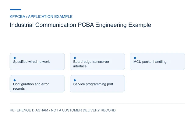
Illustrative engineering application example, not a KFPCBA customer delivery or measured production record. The configuration, calculations and record examples below are hypothetical planning inputs requiring project-specific review.
Requirements for an industrial communication controller
This example considers a controller communicating with several external equipment nodes over a specified wired link. It separates the transceiver, application protocol, power input and board-edge connectors. The label industrial communication does not select RS-485, Ethernet, CAN or any protocol. The product owner must supply the topology, cable arrangement, node roles, traffic pattern, addressing rules and expected behavior when a node is absent.
For the reference below, assume a half-duplex RS-485 physical link carrying a custom UART packet format. It is not presented as a Modbus implementation. A real Modbus or other named protocol requires its own specification, conformance scope and timing rules. Define message ownership, firmware compatibility and commissioning responsibilities before choosing a connector or declaring a board interchangeable with existing equipment.
Design constraints and the physical-layer decision
The TI THVD1450 documentation identifies a half-duplex RS-485 transceiver. That is evidence for a possible physical-interface block, not proof of application-protocol compatibility. The reference component is non-isolated; whether an installation needs galvanic isolation, additional protection or a different interface requires a separate system-level review. No isolation or compliance rating is assigned here.
Document where termination and bias components belong for the actual network rather than fitting the same option on every node by default. Define the signal reference, shield treatment, connector pin order and driver-enable behavior. A connector label such as A or B can be interpreted differently by equipment suppliers, so include functional signal definitions and a verified mating drawing. Review board-edge position against the enclosure cutout and plug-retention space.
Reference configuration and a packet-time calculation
| Block | Reference responsibility | Controlled input |
|---|---|---|
| Link interface | Transmit and receive the selected differential signals | Cable, topology and option population |
| MCU and protocol | Validate packets, address nodes and record errors | Packet specification and firmware revision |
| Board-edge hardware | Present accessible, retained connections | Mating connector and enclosure drawing |
| Service interface | Program and retrieve diagnostics | Access and recovery procedure |
Hypothetical calculation: assume a custom transaction contains a 16-byte request and a 32-byte response at 115,200 bit/s, using ten transmitted bits per byte. Serialization takes (16 + 32) × 10 ÷ 115,200 = 0.004167 s, approximately 4.17 ms. For ten nodes plus an assumed 2 ms turnaround allowance per node, a nominal scan takes 10 × (4.167 + 2) = 61.67 ms. Retries and software delays are additional; this is not a protocol-guaranteed cycle time.
Assembly and procurement choices
Release distinct BOM options for terminated endpoints and intermediate nodes if the design uses that approach. Mark option resistors and links by function, not only by reference designator. A transceiver alternate must be reviewed for supply, logic compatibility, pinout, timing and installed-network behavior. A footprint match does not preserve these characteristics automatically.
Check board-edge connectors for seating, locating pins, fasteners and mating access. The enclosure can prevent full engagement even when a connector is correctly soldered. Include the mating plug in first-article fit review when it is part of the requested scope. Communication-interface PCBA prototyping should state whether the activity covers soldered-board checks, enclosure fit, firmware loading or network integration.
Verification matrix for the link and controller
| Condition | Method | Required record |
|---|---|---|
| Known packet exchange | Use an agreed peer and packet set | Payload, node address, response and firmware versions |
| Malformed or missing packet | Inject defined errors or pause a peer | Error counter, timeout and recovery behavior |
| Transmit-to-receive transition | Capture enable timing and bus activity | Waveform, fixture and packet boundary |
| Connector installation | Mate the specified plug in the enclosure fixture | Fit, retention and pin mapping observations |
Use representative cable arrangements for the agreed link check. A short loopback cable can detect some assembly faults but does not establish a full installation distance, node count or electromagnetic compatibility result. Discuss fixture design and acceptance limits through the product-test scope, with application-protocol validation and environmental testing separately identified.
Handoff documents and a link-event record
The release package should contain PCB data, BOM options, placement and assembly files, connector drawings, cable definition, protocol specification, firmware hash, configuration image and test procedure. Include default addresses, duplicate-address handling and the recovery path after interrupted programming. A released packet dictionary helps prevent a new firmware field from being interpreted as an old one.
A proposed record is: board serial; assembly option; transceiver part; firmware hash; peer version; topology ID; packet ID; transmit time; response time; error counter; disposition. Leave unperformed checks explicitly unevaluated. Use the engineering RFQ to allocate component sourcing, programming, enclosure assembly and multi-node validation responsibilities.
Three planning scenarios
A local loopback passes but the installed network fails. What should be compared?
Compare topology, termination population, cable, signal reference, node roles and enable timing with the bench fixture. Preserve raw traffic and error counters before changing several network variables together.
A replacement board has the same connector and baud rate. Is it compatible?
Not necessarily. Verify pin functions, electrical interface, packet format, addressing, timing and firmware behavior. Mechanical fit and a shared baud rate cover only part of the interface contract.
Can every board receive the same termination components?
Only if the approved network design calls for it. Document node position and assembly options so procurement, soldering and commissioning do not independently choose conflicting configurations.
Source material and applicable scope
- Texas Instruments THVD1450 product documentation. Checked 11 November 2026. The public product details identify half-duplex operation and list the component as non-isolated; a physical-layer device does not supply an application protocol or establish installed-network performance. Applies to the half-duplex, non-isolated RS-485 transceiver reference. This source does not document a KFPCBA build, production result, approved BOM or complete-product compliance.