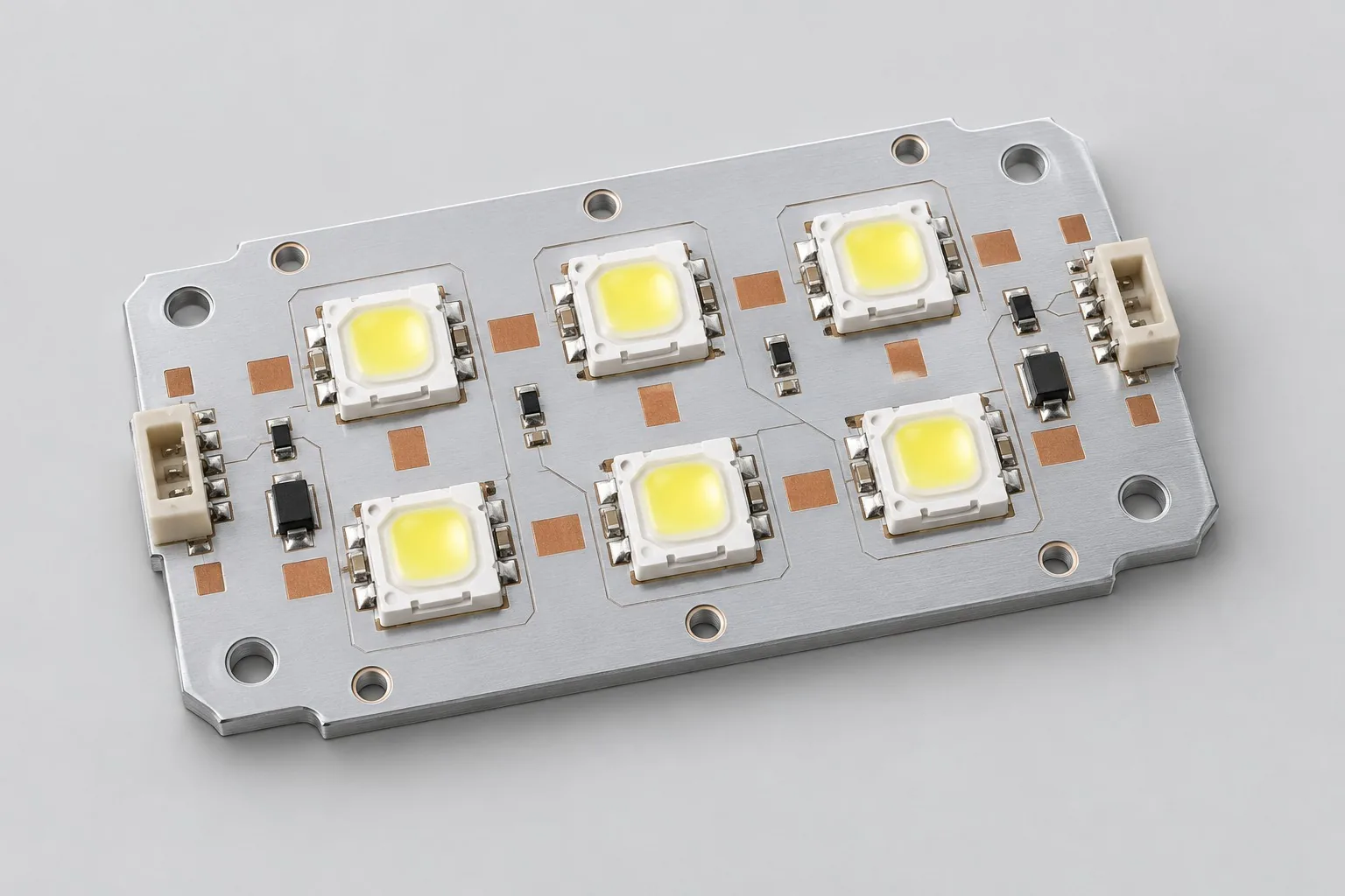
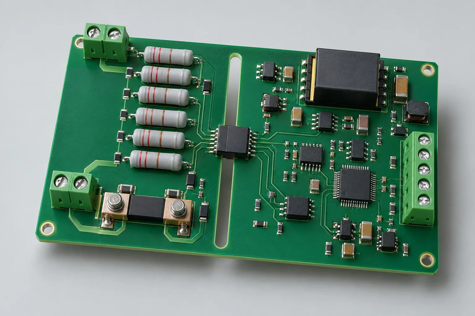
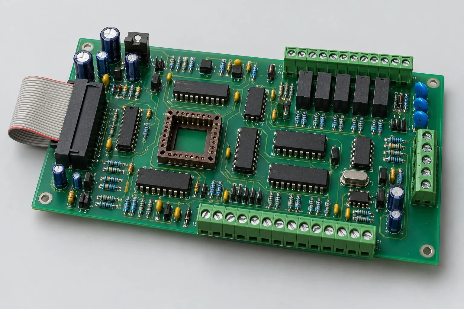
Compare design directions by product function, then define the required inputs, source-file deliverables, and prototype-acceptance method.
ELECTRONICS DESIGN · FROM REQUIREMENTS TO PROTOTYPE
Choose a Design Path for Your Product
Start with circuit, interface, and mechanical requirements, then compare the design inputs, stage deliverables, tradeoffs, and prototype-verification approach.
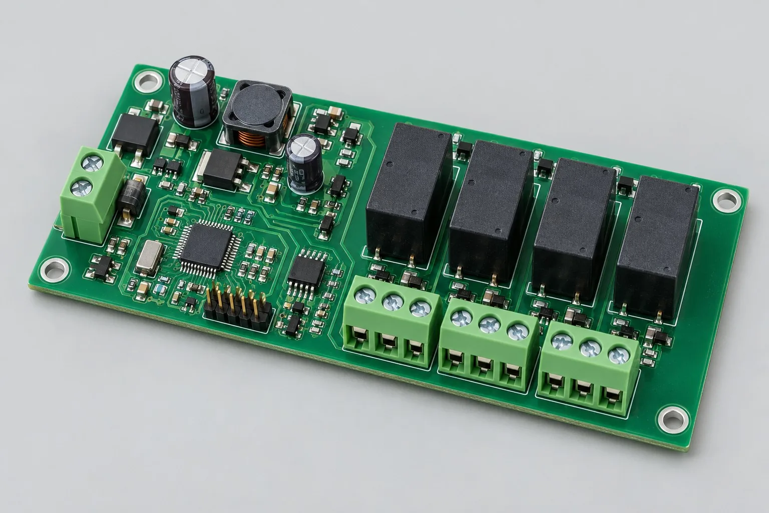
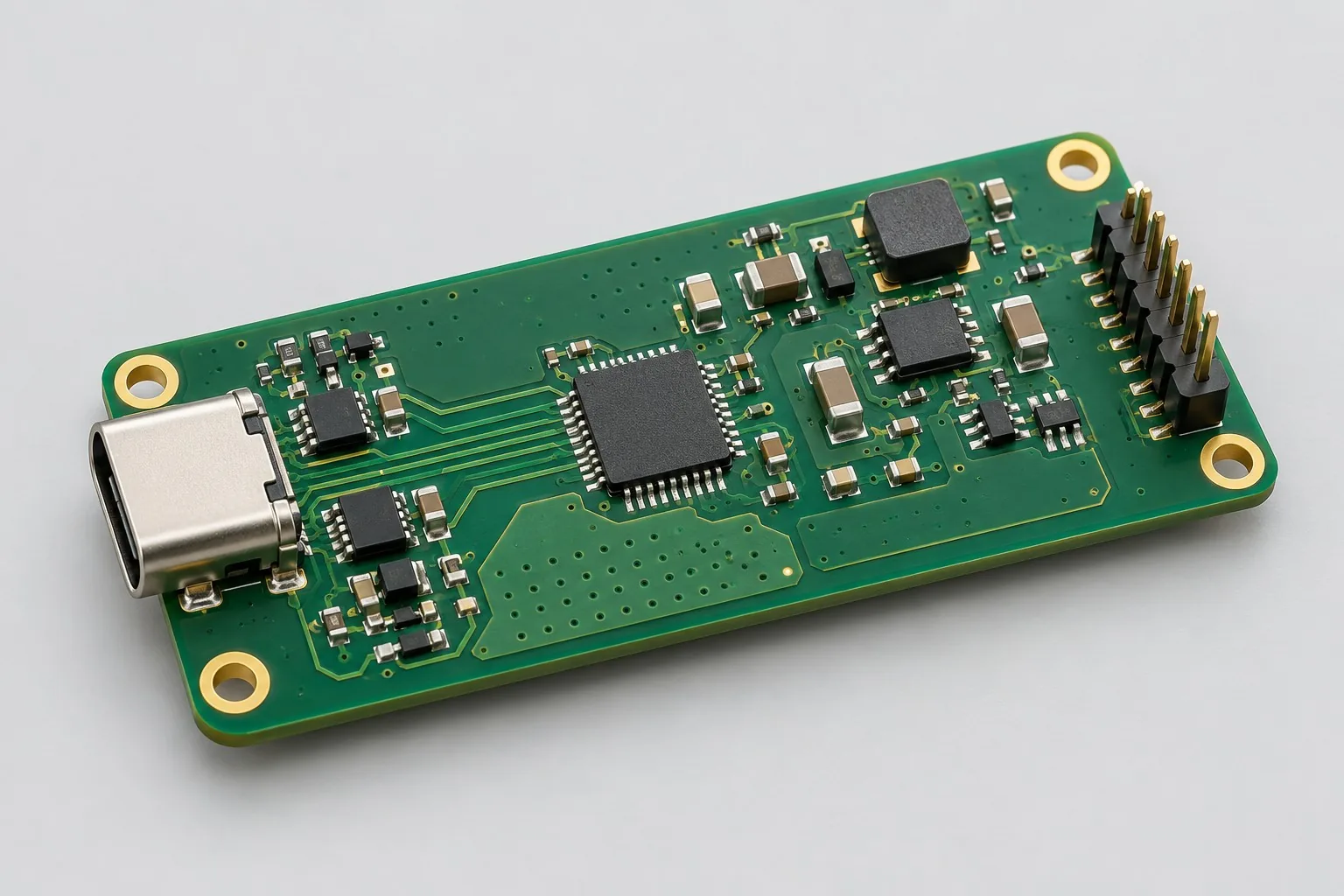
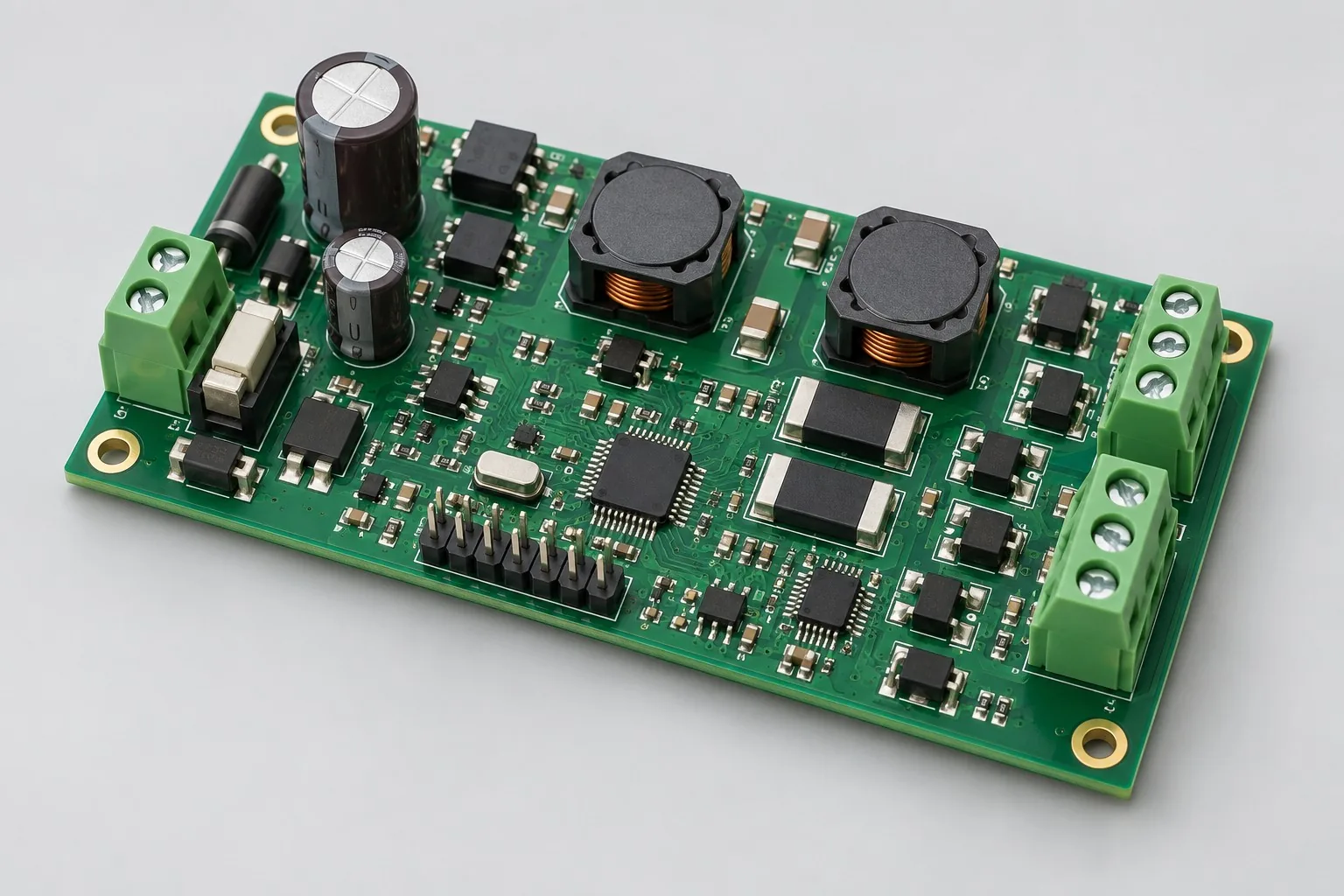
Plan single- and double-sided PCB layouts around power, routing and connector placement. Define relay loads, fault states and the manufacturing handoff.
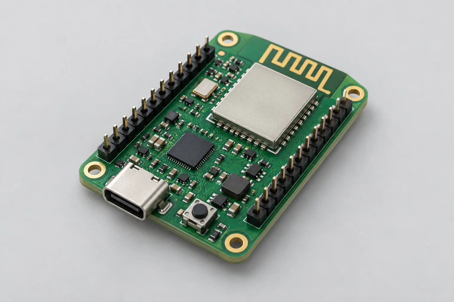
Choose an HDI design approach using package breakout, board outline and routing density. Coordinate microvias, antennas, batteries and fabrication constraints.
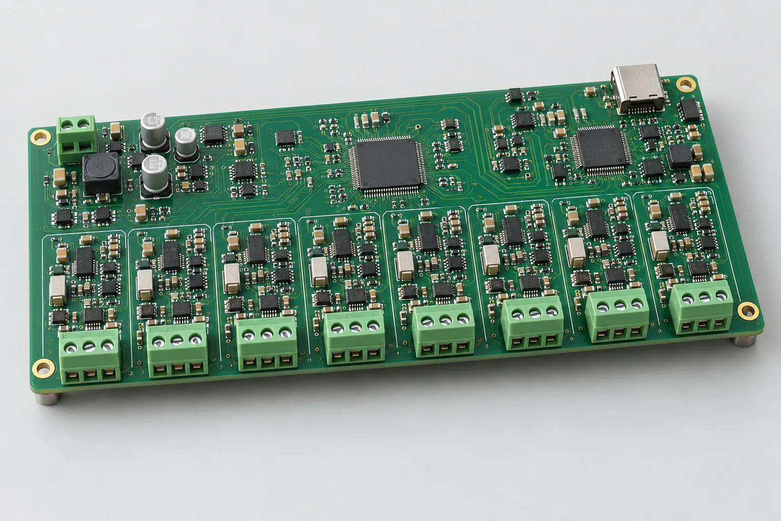
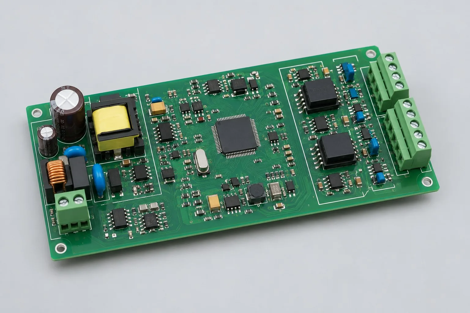
Plan multilayer PCB design for acquisition, industrial Ethernet and current-loop circuits. Define reference planes, isolation, clocks and calibration needs.
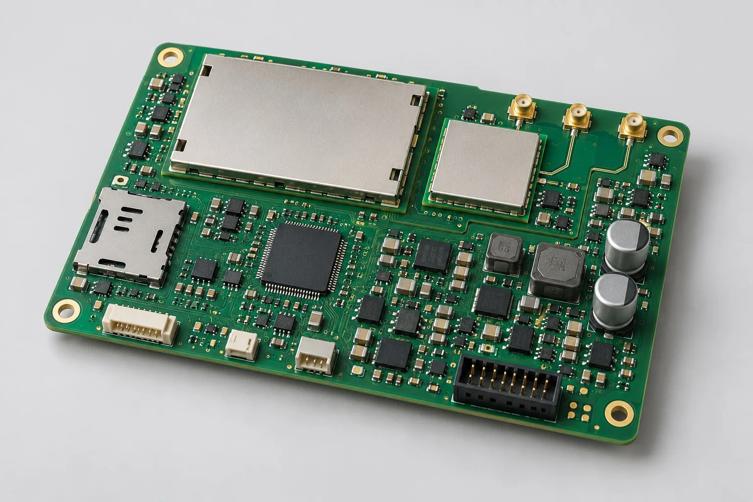
Review RF layout for positioning and wireless boards. Coordinate antennas, power, grounding, coexistence and test connections within the mechanical envelope.
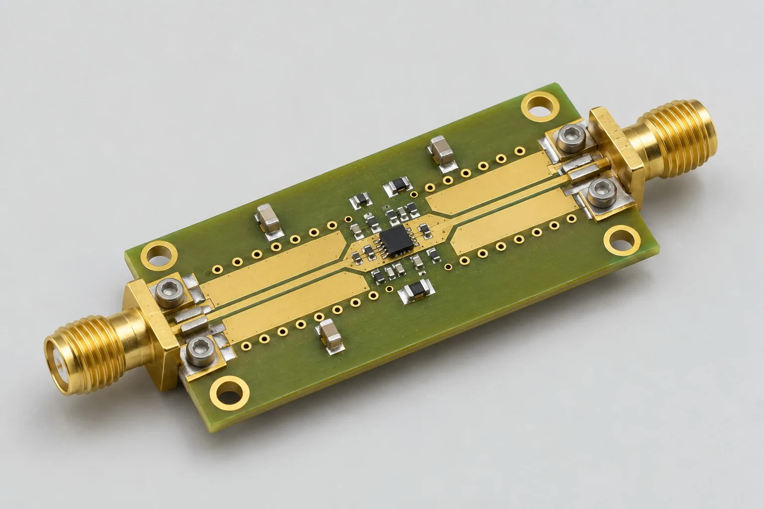
Plan amplifier PCB design around operating band, gain, bias, matching and thermal conditions. Define stability and compression tests for the prototype.
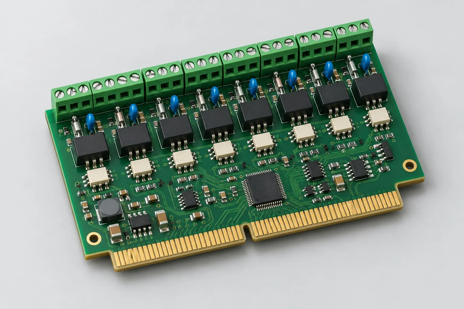
Plan gold-finger PCB layouts using the baseboard pinout, contact geometry and current requirements. Coordinate mechanics, signal conditioning and validation.
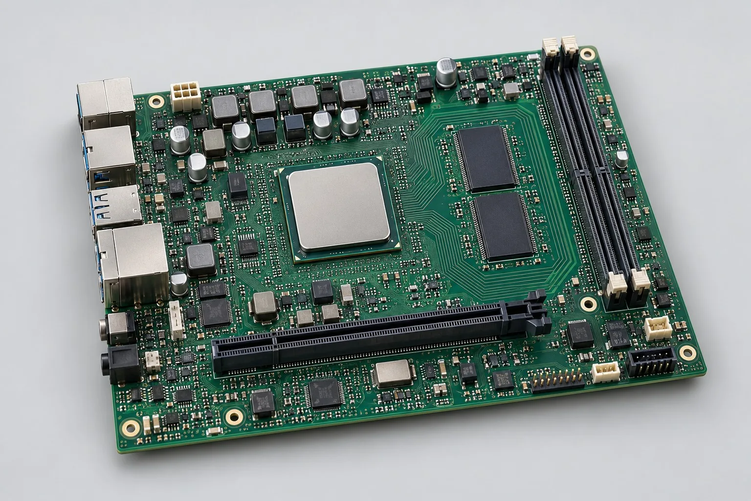
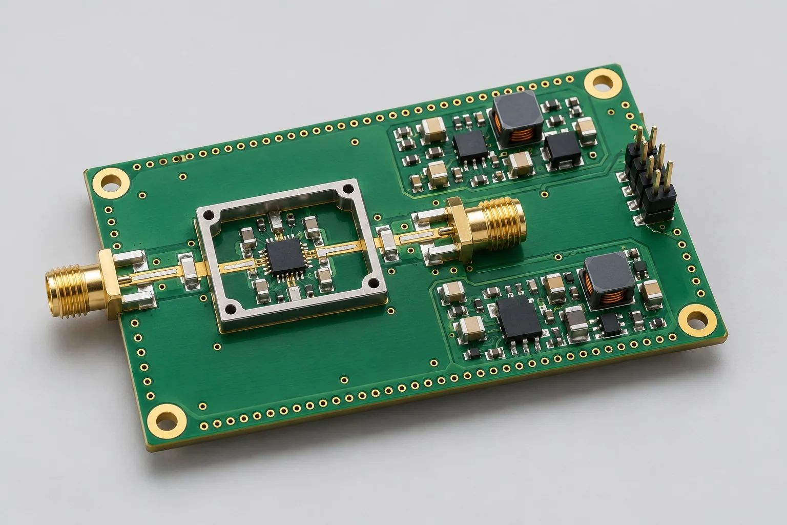
Define impedance-controlled PCB layouts using interface requirements, stackup and geometry. Coordinate routing constraints with fabrication and validation.
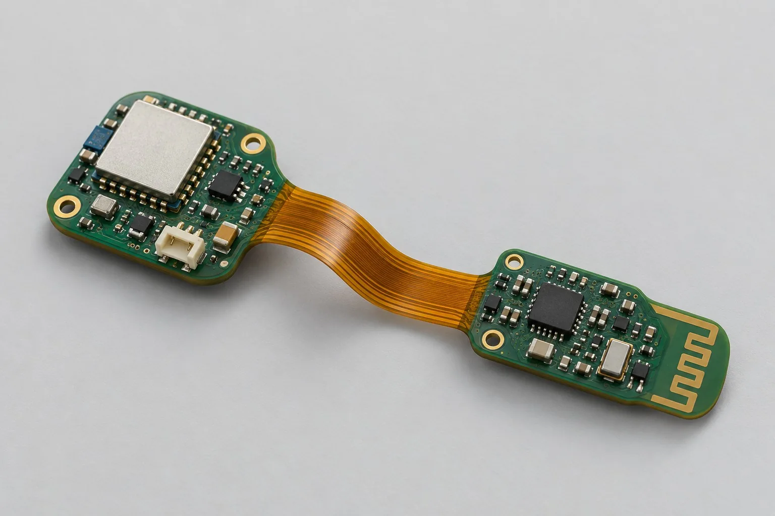
Plan rigid-flex PCB design around bend location, forming cycles, interconnects and reinforcement. Distinguish static installation from repeated flexing.
Specify halogen-free PCB materials through the exact grade, declaration scope and stackup. Review electrical and thermal requirements alongside compliance.
Share the functional target, power requirements, interfaces, mechanical constraints, current files, and the stage you want to complete so the engineering scope can be defined.
PCB design: where should electronics development begin?
PCB design and electronics development begin with functions, power, interfaces, and mechanical space. Projects with existing schematics can commission PCB placement and routing. Control board development also requires defined component selection, firmware, prototype, and test scope. Communication, acquisition, and lighting solutions are development references; performance is verified on prototypes.
Start from Function
Provide inputs and outputs, power, interfaces, mechanical requirements, and performance targets. Deliver requirements specifications, system architecture, and a component strategy before detailed design.
Start from Existing Design
Provide editable schematics, BOM, and constraints. Check footprints, power, interfaces, and fabrication conditions before completing the layout and manufacturing files.
Start from Prototype Issues
Provide the original board, revision, reproducible operating conditions, and waveforms/logs. Locate the bottleneck first, create a revision and regression plan, then deliver the new revision.
How much does PCB design cost? First check the work included in the quote
PCB design is quoted by scope and complexity, not board area alone. For layout from existing schematics, compare footprints, layer order, net constraints, and mechanical requirements. Starting from functions also requires architecture, component selection, and circuit development. List software, prototype build, instrument testing, and subsequent changes separately to compare two total quotes.
Quotation terms depend on the approved files, quantity, material supply, tests and delivery requirements.
Footprints, placement, routing, and manufacturing files for an existing circuit
Whether the customer supplies schematics and firmware, and whether critical net analysis is included
Circuit and System Development
Architecture, power, interfaces, component selection, and schematics
Whether functions, operating conditions, and editable source files are in the same scope
Software and Integration
Firmware, communication, host, or application side
Which endpoints are developed, and who owns protocols and fault recovery
Prototype Preparation and Verification
Bare PCBs, materials, assembly, instruments, and testing
How unit count, test conditions, and subsequent corrections are included
How do I choose layout, control board development, or a complete solution?
Layout implements a defined circuit and its constraints on a PCB. Complete development also addresses functional architecture, power, interfaces, components, and software. If an existing circuit is unverified, routing alone cannot constitute complete product development; first confirm schematic responsibility and verification scope.
Choose the route by routing density, reference planes, power, component breakout, and mechanical requirements. Compare single- and double-sided boards for conventional control, check multilayer reference planes for multichannel and high-speed interfaces, and consider HDI only when compact packages actually need microvias. Increasing or reducing layer count requires a functional basis.
Compare project directions: relay and low-voltage control, synchronous acquisition and industrial control, positioning and wireless communication, and constant-current LED drive and color mixing. The individual pages explain configurations, quote boundaries, and prototype evaluation methods.
Circuit development phase delivery
phase
Primary Tasks
Reviewable Deliverables
Requirements and Architecture
Define functions, interfaces, states, and performance conditions
Requirements specifications, functional architecture, component selection, and issue list
Schematic and layout
Component selection, power, footprints, stackup, constraints, and mechanical coordination
Editable source files, BOM, stackup/net constraints, and review records
Manufacturing and Assembly
Joint bare PCB and PCB assembly review, file freeze, and substitute part verification
Gerber/drill files, BOM, pick-and-place files, assembly drawings, and programming/test package
Prototypes and Closure
Measure under agreed conditions, reproduce faults, and close changes
Test methods and raw results, issue list, approved revisions, and limitations
Specify these details before quoting
State the required product functions, inputs and outputs, power and interfaces, whether the board outline and mechanical design are fixed, which files exist, and the desired delivery stage. Agree separately on firmware, mobile/cloud systems, mechanical design, fixtures, and certification work so development boundaries are clear within the design fee.
Ensure design and manufacturing use the same version
Resolve critical materials, stackup, footprints, substitute components, and test points jointly in PCB and PCB assembly reviews. Revision records must link requirements, design files, manufacturing packages, and software revisions. Retain models and assumptions for calculations and simulations, and record test conditions and exclusions in prototype reports.
Common questions on design quotation and component selection
How much does PCB design cost, and what determines the fees?
A project-specific quotation requires review of the available files, quantity, materials, requested tests, delivery destination, taxes, shipping, and trade terms. Complete development separately prices circuits, firmware, prototypes, and verification. Any formula on this page organizes cost inputs; it is not a quoted rate.View cost items, calculation conditions, and sources.
How does PCB layout differ from complete circuit board development?
Layout implements a defined circuit and its constraints on a PCB. Complete development also addresses functional architecture, power, interfaces, components, and software.
Do PCB design fees include fabrication, SMT assembly, and components?
List design investment separately from prototype manufacturing costs. When comparing quotes, check whether bare PCBs, BOM procurement, SMT/DIP, programming, and prototype quantities are included. Even when one quote covers several stages, examine the breakdown to avoid confusing one-time development fees with per-batch assembly fees.
How to choose a PCB design manufacturer?
First check whether the provider can explain architecture tradeoffs, critical constraints, and verification methods for the specific project, then confirm delivery scope for editable source files, BOM, manufacturing files, and software. Communication, analog acquisition, power, and RF projects require different criteria; do not decide solely by the lowest price or an attractive board layout.
How do I choose a two-layer, four-layer, or HDI design?
Choose the route by routing density, reference planes, power, component breakout, and mechanical requirements.
Does an electronics development quote include the app and cloud services?
Board hardware, firmware, host software, mobile apps, and cloud services are separate deliverables. For an end-to-end system, list protocols, operating states, fault recovery, and integration endpoints. A hardware-only development quote does not automatically include all application software.
What primarily affects prototype development time?
Critical component availability, mechanical design freeze, bare PCB processes, software interfaces, and measurement conditions all affect scheduling. Verify higher-risk power, signal, or mechanical paths first, then complete other functions. Adjust verification when requirements or components change; layer count alone cannot establish a fixed number of days.
Can I get a PCB development budget before the functional requirements are complete?
Start by describing what the product does, its operating environment or application, power supply, main interfaces, and available files to assess the requirements/architecture phase. Qualify the budget around unresolved inputs, then freeze the circuit, software, and prototype. Initial consultation does not require every design file, but undefined functions cannot receive a fixed all-inclusive price.
How should a budget separate one-time development and per-batch manufacturing?
List requirements, circuit design, layout, firmware, and verification under one-time development. List bare PCBs, BOM, assembly, and unit count under prototype builds. Quote subsequent batches separately by manufacturing quantity and test scope. Compare all three lists against the same requirements revision. Do not treat SMT per-point pricing as development pricing or an amortized development figure as a stable per-unit purchasing price.
Can I purchase only design modifications if I already have Gerber files and a BOM?
First confirm whether editable schematics/PCB files, net constraints, and software revisions are available. Manufacturing files support checking but are not complete source files. Mechanical, interface, or power changes may require additional file recovery. Define review, local revision, and new development as distinct scopes; Gerber availability does not remove circuit responsibility.
How should an electronics development quote define firmware maintainability?
Specify commissioned endpoints, source code and build environment, third-party library licenses, configuration, and programming/recovery tools. Binary-only delivery differs from editable source delivery. If the customer supplies existing firmware, agree on modification rights and new-board regression scope so later maintenance does not depend on undisclosed tools.
Must design source files be delivered with the manufacturing package?
Define the scope of source files, libraries, BOM, mechanical/stackup constraints, and manufacturing package in the agreement. Gerber, drill, and pick-and-place files support production, while schematic/PCB source files support maintenance; link them to the same revision. Separately specify rights and deliverable scope for software, models, and third-party tools. Payment does not automatically convey all intellectual property.
How are prototype corrections priced differently from new requirements?
Use approved requirements and acceptance cases to distinguish troubleshooting/corrections for unmet original targets from customer requests for added interfaces, mechanical changes, or higher performance. Agree on revision rounds, impact review, and regression scope before quoting. Do not imply unconfirmed commitments to unlimited free revisions or guaranteed test acceptance.
Which development tasks can reuse from an earlier project reduce?
First list revisions and interface conditions for circuit, software, mechanical, and tool modules. Confirmed reusable portions reduce duplicate development, but new loads, input measurement ranges, antennas, or assemblies still require verification. Historical development directions do not mean reference parameters were delivered in production, and a similar product name does not prove direct reuse is possible.
How do I check for omissions in a low design quote?
Against the same requirements revision, check schematic responsibility, component selection, net constraints, source code, prototype count, and actual test targets. Focus on exclusions and third-party endpoints, and compare scope through deliverable files and acceptance records. Do not choose solely by total price, board appearance, or generalized capability claims.
Should I build a proof-of-concept prototype before a complete mainboard?
When peak power, analog error, wireless/antenna behavior, or mechanical feedback remains uncertain, use a measurable proof-of-concept prototype to resolve high risks first. Then freeze the mechanical design and final PCB. Record which temporary circuits can be reused and which need rerouting in the budget. A working proof of concept does not mean the production revision or complete product testing is finished.
Can design fees include product certification?
Define certification targets, submitted samples, corrective work, and third-party fees separately. Design or EMI prechecks do not automatically complete certification. Confirm applicable project conditions first, then agree on engineering support and test boundaries. Do not promise fixed fees, passing results, or schedules without a clear source.
What additional engineering work is needed to move from prototypes to low-volume production?
Freeze matching hardware, BOM, firmware, and manufacturing packages. Review substitutes, programming/calibration, test points, and production criteria. Select load, data, RF, or optical inspections by product, and define development acceptance separately from production screening. Prototype acceptance does not eliminate low-volume manufacturing and revision control.
Agree staged deliverables before development
Work area
Inputs or responsibility
Expected output
Layout only
Approved schematic and mechanics
Board source, agreed libraries and manufacturing outputs
Hardware development
Requirement and electrical boundaries
Schematic, BOM, layout and verification scope
Hardware and firmware
Behavior, interfaces and software boundaries
Build instructions, source and binaries as agreed
Production introduction
Approved revisions and known issues
Programming, test, manufacturing and change-control handoff
Use the development scope and cost comparison to prepare the discussion. Unknown inputs should be listed as open questions; they do not authorize substitutions, omitted tests or unrecorded design changes.
PCB / PCBA · PROJECT ENQUIRY
Does Your Project Need PCB Fabrication, Assembly, or Box Build?
Tell us the product use and which files are available. We can define the next engineering step even when the data package is not complete.