
Prototype Phase
Build calibrated measurement chains by band, rate, and port to verify RF/wired channels and enclosure shielding effects.
For wireless transceivers, gateways, and high-speed interface boards, jointly review high-frequency materials, impedance, RF partitioning, shielding, and channel test conditions.
Request Communication Board Assembly →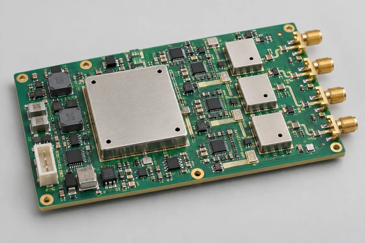
| Project Direction | PCB Manufacturing and Layout Focus | PCBA assembly and testing highlights |
|---|---|---|
| Multi-band wireless transceiver module | RF materials/stackup, feedline impedance, filtering, and shielding boundaries | Transmit/receive operation in each band, power/frequency conditions, and calibration files |
| Wired communication gateway board | Differential trace reference planes, magnetic components, isolation, and interface protection | Interface rates, throughput conditions, long-duration transmission/reception, and reconnection |
| High-speed acquisition and communication board | Clock distribution, BGA fanout, vias, and backdrilling | Startup, channel consistency, continuous transmission, and temperature rise |
| Review Items | What specific inputs are provided | How to confirm results |
|---|---|---|
| Material and Impedance | Frequency, material grade, dielectric thickness/copper weight, impedance targets, and test coupons | Freeze stackup and impedance compensation approvals; high frequency is not a single material name |
| RF Assembly | Shields, RF connectors, solder, and cleanability | Check pads, shield grounding, and rework access to prevent contamination from affecting RF performance |
| Test Interface | Test ports, calibration standards, cable losses, and test bands/bandwidth | Retain calibration status, power conditions, and test revisions. Do not extend single-frequency results to the full band |
Build calibrated measurement chains by band, rate, and port to verify RF/wired channels and enclosure shielding effects.
Freeze cable compensation, test reference planes, firmware, and continuous transmission conditions. Close shield rework and fixture contact issues.
Deliver against the approved band and channel matrix, retaining calibration status, transmit/receive results, and thermal records. List untested bands separately.
For network communication projects, provide Gerber files, drills, BOM, pick-and-place files, and assembly drawings, plus operating environment, actual interfaces/loads, enclosure and harness drawings, target quantity, and the test limits above. If programming or calibration is commissioned, add firmware revision, checksum, fixture wiring, and writing permissions.
Agree separately on port, power, calibration, and software conditions for board-level transmission/reception, complete product antennas, and system throughput.
View specific fabrication products by board-level task, or arrange a joint PCB fabrication and assembly review with complete information.
Engineering reference | QFN and SON assembly: thermal pads, printing, and solder joint verification: QFN/SON pad, stencil, and measured thermal process methods; not company capabilities.
Engineering reference | Packaging PCB fabrication files: units, layer order, and engineering notes: methods for PCB fabrication, hole layer spans, and file semantics.

Tell us the product use and which files are available. We can define the next engineering step even when the data package is not complete.