
RF transceiver gain and bias board design
This page uses a gain module as a front end and does not describe it as a complete high-power PA; higher power requires separate power-device selection and output matching.
Distinguish RF gain/bias from stereo Class D audio output. Design for signal, load, distortion, and thermal conditions, and deliver prototype validation for the applicable revision. Separate RF gain/bias amplifiers from audio power-output amplifiers, establishing signal-quality, load, and thermal budgets for each.
Configurations in this category support development requirements discussions. Actual components, structures, and performance are confirmed in the project revision; historical development directions and engineering references are identified separately.
This category covers RF gain and Class D audio amplifiers. Costs are broken down by schematic, PCB layout, agreed software, and prototype validation scope; the main workload differences involve bias or output filtering, thermal design, and RF/audio load testing. Layer count, board area, or channel count alone cannot determine development pricing; the usability of existing files and test conditions also affect the effort.
Quotation terms depend on the approved files, quantity, material supply, tests and delivery requirements.
Prepare a structured RFQ or use the short inquiry form.
| Quotation Items | What services are included | What to Check When Comparing Quotes |
|---|---|---|
| Existing circuit layout | Implement layout using approved schematics, footprints, and mechanical design | Whether schematic review, stackup/constraints, and fabrication files are included |
| From functional R&D | Bias or output filtering, thermal design, and RF/audio load testing | Whether circuits, firmware, and validation targets are complete |
| Prototypes and revisions | Build prototypes from the frozen design, record test feedback, and release a controlled revision | Whether prototype quantity, component procurement, and change scope use the same basis |
RF designs focus on bands, matching, and gain/compression; audio designs focus on speaker loads, distortion, noise, and cooling. Compare costs using each design's measurement tasks, rather than output power alone.
Start selection with input level, load, continuous power, and supply, then review the parameters, cost boundaries, and validation conditions of the specific designs below.
| Review Questions | Why it impacts design | How to select and close |
|---|---|---|
| RF and audio | RF focuses on matching, stability, and linearity; audio focuses on load, filtering, distortion, and protection. | Select components and topology by application; do not present peak output or component typical values as whole-board guarantees. |
| Power supply and bias | Supply noise and bias changes affect output. | Define supply headroom, power-on sequencing, enable control, and abnormal shutdown, and retain measurement points. |
| Power and heat dissipation | Load, frequency, and cooling conditions affect sustainable output. | Check losses and the thermal path, then specify test load, duration, and temperature-rise criteria. |
RF band or audio bandwidth, gain/output targets, input level, load, supply, efficiency, and cooling structure.
| Current Stage | Customer-Supplied Materials | Design deliverables |
|---|---|---|
| Functional requirements only | RF band or audio bandwidth, gain/output targets, input level, load, supply, efficiency, and cooling structure. | Functional/state requirements, approach comparison, mechanical design, and open items for RF front ends and audio outputs |
| Existing schematics or PCB | Editable circuit/PCB files, BOM, and mechanical design for products in this category; include RF band or audio bandwidth, gain/output targets, input level, load, supply, efficiency, and cooling structure. | Signal chain, bias/power budgets, thermal layout, load conditions, and test records |
| Existing prototype pending revision | Fault reproduction conditions, raw logs/waveforms, test equipment, and original board revision | Troubleshoot faults related to RF front ends and audio outputs, and deliver revised files, an impact list, and regression records under the same operating conditions |
This page uses a gain module as a front end and does not describe it as a complete high-power PA; higher power requires separate power-device selection and output matching.
Differential inputs help manage common-mode noise; single-ended inputs require defined signal ground and gain.
Signal chain, bias/power budgets, thermal layout, load conditions, and test records. Link deliverables to the same requirements revision; the PCB fabricator confirms materials, stackup, holes, and fabrication conditions, while PCB assembly checks footprints, soldering, programming, and test points. Recheck this category's constraints after critical-component substitutions or mechanical changes.
Key validation in this category: load and output, band/gain or distortion, efficiency and temperature rise, protection, and fault recovery.
| Acceptance Stage | Conditions to be frozen | Report Records |
|---|---|---|
| Functionality and boundaries | Component/software revisions, supply/load, and interface or mechanical operating conditions | Test procedures, raw logs/waveforms, results, and abnormal states |
| Application-specific performance | Load and output, band/gain or distortion, efficiency and temperature rise, protection, and fault recovery | Instruments and calibration, environment, samples, criteria, and exclusions |
| Version Closure | Change list, permitted limitations, passed items, and open items | Fabrication and software packages, test reports, and issue-closure records |
RF designs focus on bands, matching, and gain/compression; audio designs focus on speaker loads, distortion, noise, and cooling.
First specify input level, load, continuous power, and supply.
Layout-only work can be discussed when usable schematics and component information exist. Starting from RF-gain or Class D audio-amplifier requirements requires selection and circuit design first. Itemize software, prototypes, and testing separately; do not treat layout fees as a complete development budget.
For RF gain, list frequency band/input level, bias matching, compression, and stability; for Class D audio, list speakers, LC filters, distortion, noise floor, and thermal conditions. Compare quotations using each design's supply and continuous operating conditions; gain in dB and speaker wattage are different procurement bases.
For RF, provide source/load and reference planes; for audio, provide speaker impedance and cables. Both require components, bias/power, and cooling installation details. Complete circuit development first if matching, output filtering, or protection is unresolved; thermal-pad layout cannot replace continuous-power validation.
A basic board for fixed analog audio or fixed-bias RF may require no MCU firmware. If mute/shutdown, temperature/current monitoring, and fault recovery are needed, define endpoints and timing; existing customer control tools may be reusable. An output signal does not establish completion of all control and protection functions.
Retain the actual matching/filter BOM, load, gain or current settings, thermal path, and hardware source files. Include timing/thresholds in the control package and band/level or distortion/load conditions in test records. Review linearity and cooling before increasing output, rather than only changing advertised power.
Check component operating limits, bias, power devices, filters, protection, and cooling, then retest for the RF or audio task. Specify reusable input/control portions; output, distortion/compression, and temperature rise require new validation. A voltage increase does not automatically increase usable power.
Band, operating level, load, and filtering determine suitability; an RF front end cannot become an audio output stage. Power/thermal review methods are reusable, while specific components and tests must be revisited by product; typical IC specifications cannot replace a whole-board guarantee for new equipment.
Initially describe the product task, application, and current files. A formal quotation should confirm RF band or audio bandwidth, gain/output targets, input level, load, supply, efficiency, and cooling structure. If source files exist, provide circuit/PCB/BOM and mechanical revisions together; if prototypes exist, include fault conditions. First identify frozen functions and structures, then compare circuit, layout, software, and validation work; unresolved items must not be assumed to share the same service scope.
Key validation in this category: load and output, band/gain or distortion, efficiency and temperature rise, protection, and fault recovery. For each RFQ item, specify the actual load/interface or structure, prototype quantity, measurement method, equipment, and permitted deviation; deliver raw results, anomalies, and revision closure separately. Circuit/PCB checks and complete-unit functional validation are different tasks; a quotation including only the former does not justify omitting the performance measurements specific to this category.
Select and place components using the manufacturer information in the specific design details, and record file revisions and applicable conditions with the project; the company's historical development directions do not mean the reference designs on this page have been delivered in volume.
Return to the electronics design technical section · PCB Manufacturing · PCB assembly · Submit R&D requirements. When requesting power amplifier PCB design, prepare functions, interfaces, board outline, and existing design information.
Send the product functions, interfaces, mechanical constraints, available files, and required development stage. Compare design capability scope and development support before defining deliverables.
Compare reference designs by function, interfaces, and mechanical constraints, including design tradeoffs and prototype-acceptance methods.
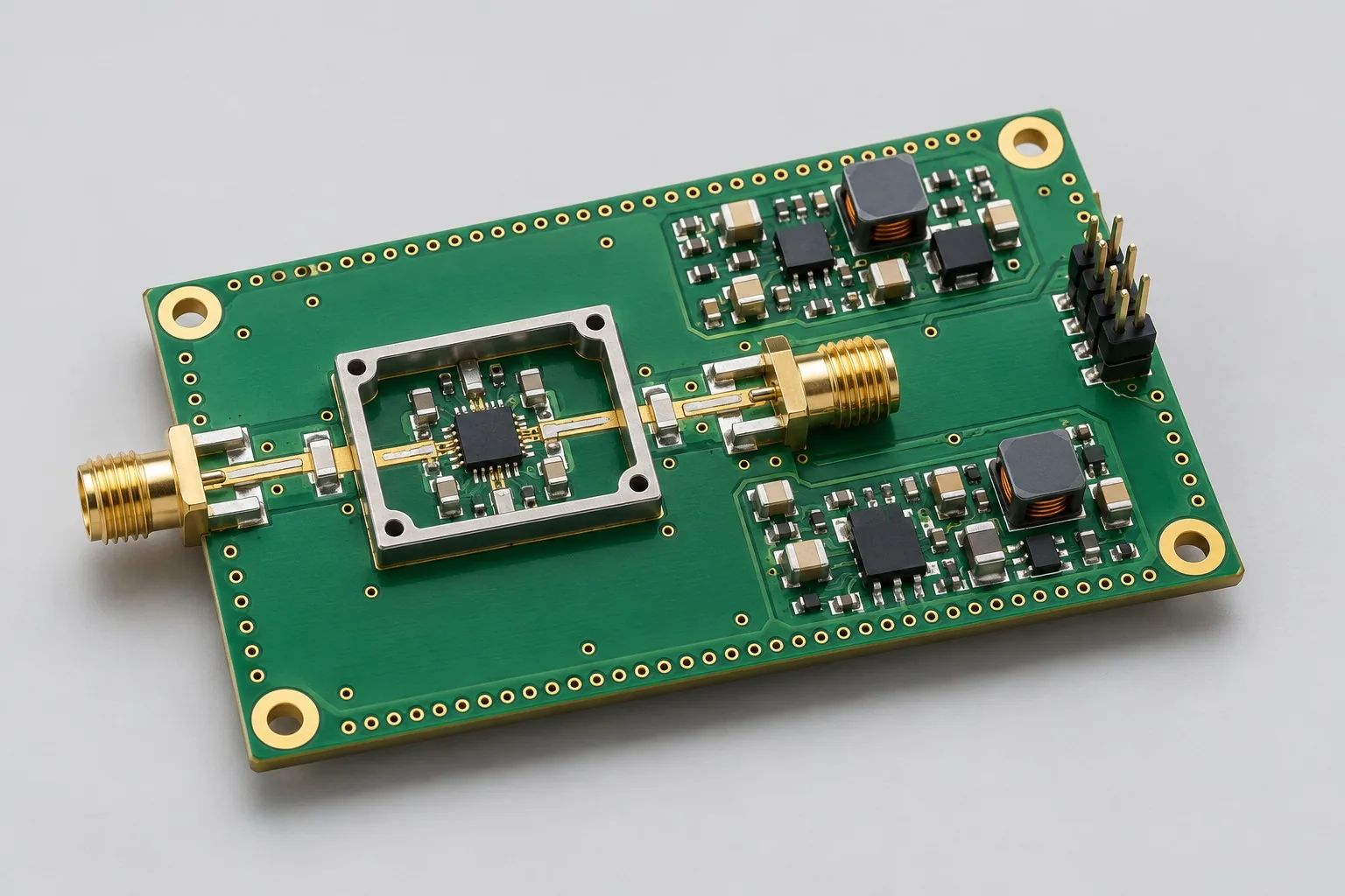
RF gain-board design: provide actual bands corresponding to the 900MHz example, input levels, target output, and power. Separate device/bias, matching-sample, and linearity/stability budgets. Itemize optional protection/temperature monitoring to distinguish ordinary front-end gain from complete transmitter power-stage scope.
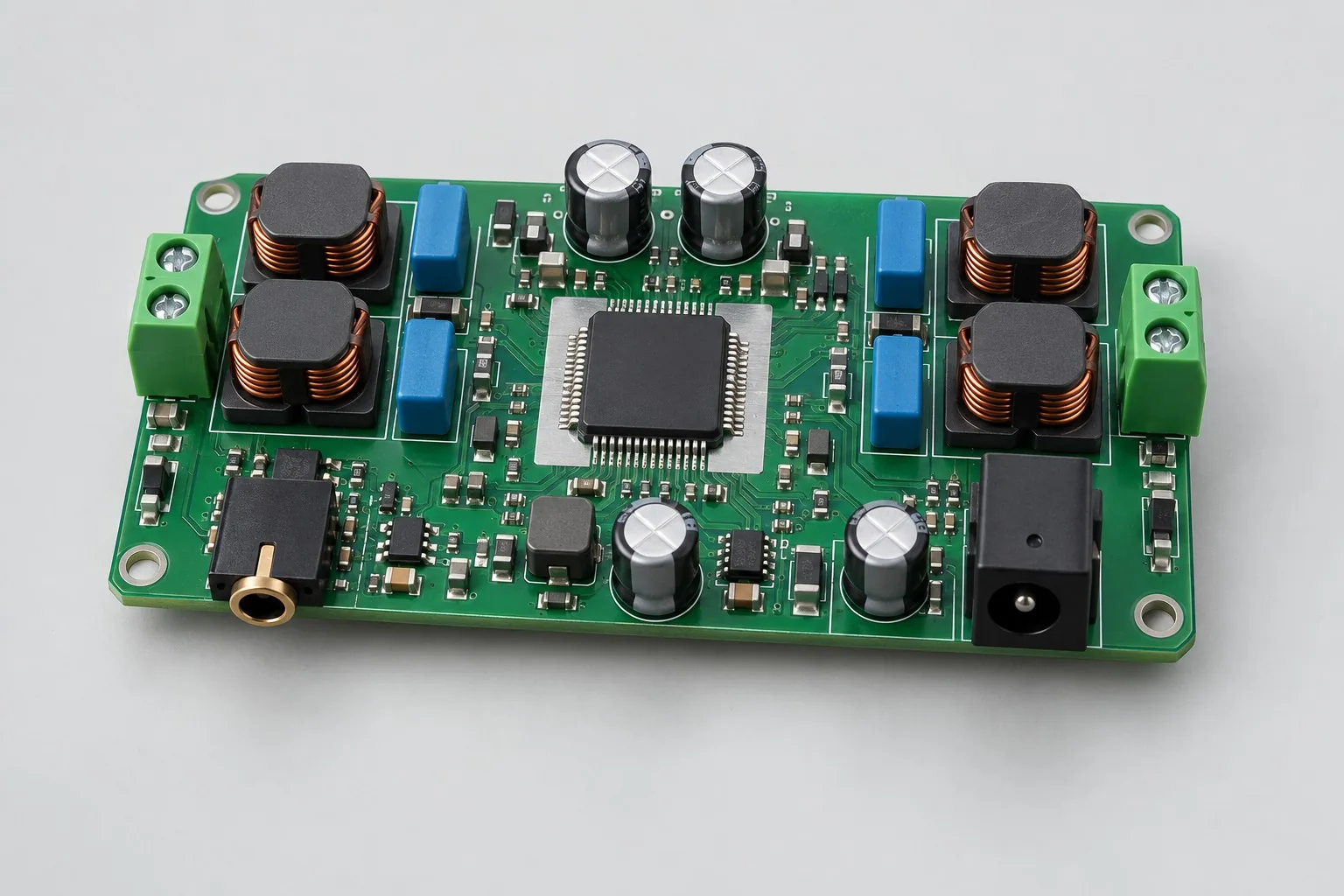
Class-D amplifier design: fix conditions using 24V, 4Ω or 8Ω versions, and the example 20W-per-channel target. Separately quote basic audio, loaded distortion/noise floor, sustained thermal tests, and EMI prescans. Identify speaker/cable providers; basic audio costs are not comparable to scope including system thermal/electromagnetic measurements.

Tell us the product use and which files are available. We can define the next engineering step even when the data package is not complete.