
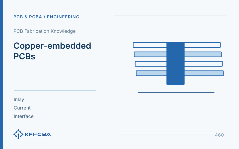
Copper embedding places copper profiles or structures locally within a multilayer PCB, allowing high-current paths and dense control circuitry to share one board. Effective cross-section, length, connection interfaces, insulation, and the heat-removal path jointly determine performance. A thick copper block does not mean the holes, pads, or terminals connected to it can carry the same load.
Trace the complete current path first
Follow the path from the input terminal through solder joints, vias or microvias, embedded copper, and output connections to the load. Specify continuous and transient current, duty cycle, and allowable temperature rise for each section. The narrowest cross-section and contact interfaces may be more sensitive than the copper block itself. If the return path uses an ordinary thin copper layer, analysis cannot cover only the forward embedded-copper path.
Würth's copper-embedding rules explain how local copper profiles in multilayer constructions can combine high current with logic routing and require dedicated core and PP combinations. This describes a structural approach; supplier-specific dimensions and material configurations must not be presented as another company's capabilities. Review the design using its actual three-dimensional construction.
Cross-section and resistance calculation examples
In an engineering example, a copper strip 5 mm wide and 0.5 mm thick has an effective cross-section A=5×0.5=2.5 mm²; a length of 30 mm equals 0.03 m. For illustration, assume resistivity at that temperature is ρ=0.0175 Ω·mm²/m. Then R=ρL/A=0.00021 Ω. At 20 A, the voltage drop is approximately 4.2 mV and resistive heating in the strip is P=I²R=0.084 W.
The resistivity here is an example assumption. The calculation excludes temperature changes, connections, hole groups, solder joints, and current crowding; it is not a current-capacity guarantee for embedded copper. If the connections add another 0.5 mΩ, they dissipate an additional 0.20 W at the same current, already exceeding the example strip's own loss. This shows why reporting copper weight alone misses bottlenecks.
What a three-dimensional structural drawing should include
| Input | Note | Related engineering tasks |
|---|---|---|
| Copper Profile Dimensions | Outline, thickness, tolerances, corner radii, and position | Cross-section, windowing, and mechanical processing |
| Intra-layer Position | Top and bottom dielectric, adjacent copper layers, and total thickness | Insulation, lamination, and alignment |
| Electrical Connection | Hole groups, pads, terminals, and reflow | Voltage drop, local temperature rise, and continuity |
| Thermal Connections | Heat source, heat dissipation surface, interface, and fixation | Complete Thermal Path |
| Verification Requirements | Load, environment, test points, and criteria source | First article and subsequent batch approval |
A copper strip's plan-view outline alone does not define the interlayer construction. Its embedded position and dielectric thickness should match the controlled stackup. Show terminals, screws, and the enclosure as well to avoid unintended contact with conductive structures after installation.
How should insulation and interlayer bonding be reviewed together?
Copper-profile edges, adjacent layers, machining boundaries, and mounting points may all affect insulation. Required spacing, dielectrics, and tests come from product requirements; do not infer a safe voltage from copper-block thickness or a material table. Copper and resin expand differently, so interfaces, fill, and local stress also require review.
Embedded copper changes local copper height differences and thermal mass. The fabricator must confirm cutouts, lamination fill, planarity, and hole-processing routes. First-article checks should include representative interfaces as well as electrical tests. A flat exterior does not prove sound internal bonding, and one local cross-section does not cover every boundary of the entire copper structure.
Comparison with thick copper and external busbars
| Solution | Comparative Benefits | Work Effort Required |
|---|---|---|
| Full-Copper Layer | Continuous copper construction with relatively straightforward local connections | Review of routing density, etching, and resin fill |
| Localized Copper Embed | Concentrate large cross-sections at required locations | Embedding, connections, lamination, and interface validation |
| External Busbar | Large current paths can be arranged independently | Connection, mounting, space, and assembly control |
Compare alternatives under the same load, allowable temperature rise, space, and insulation requirements. Do not compare price only by copper mass or thickness, and do not ignore connection and maintenance requirements for external solutions. Selection depends on system constraints, not the complexity of a technology's name.
How to measure voltage drop and temperature rise reliably?
- Define current paths and measurement points section by section for the approved load, first confirming protection and test conditions.
- Use an appropriate four-wire approach for low-resistance voltage-drop measurements, separating current leads from sense points.
- Record current, voltage drop, environment, and stabilized temperature, stating whether the measurement includes terminals and solder joints.
- Check hot spots at components, hole groups, copper blocks, and exit connections while maintaining consistent mounting conditions.
- Use cross-sections and connection records to confirm that temperature results correspond to the approved construction.
Sense points spanning a terminal include its contact resistance, while measurements only in the middle of the copper block may miss the hottest connection. Define the measurement object beforehand so R=V/I and P=VI can be recalculated later. Infrared measurements on bare copper must account for reflections and emissivity; a low reading does not necessarily mean a low temperature.
How do you troubleshoot hot connections when the copper block stays cool?
Check solder joints, hole groups, actual connection area, local current crowding, and contact pressure, measuring voltage drop separately for each. If one section's resistance increases abnormally over time at the same load, record temperature and contact changes. If only some lots are affected, check copper-profile, metallization, and assembly lots. Do not simply thicken the copper block without improving its connections.
If the copper block itself runs hot, check its cross-section, length, and heat-removal path. Analyze insulation or interface problems by location and thermal history. Record electrical, thermal, and structural findings separately in the engineering report before identifying common causes; one current-capacity number cannot replace all results.
How should construction approval and subsequent changes be defined?
Approval should be tied to three-dimensional dimensions, stackup, connection method, operating conditions, and validation scope. Later changes to terminals, hole groups, or heat sinks may affect results even when the copper block is unchanged and require review according to their effects. For repeat orders, record material lots and production routes so measurements remain traceable to actual board IDs.
For local heat transfer, also establish where the heat actually flows. Low electrical resistance does not mean low device-to-ambient thermal resistance; the copper block must connect effectively to both the heat source and the heat-removal path. Thermal and electrical validation can share structural information but have separate measurement objects and criteria.
How should continuous and pulsed loads be evaluated separately?
The load waveform determines average heating and affects local transients. The average current shown by a power supply cannot be treated as the current at every instant; resistive loss depends on current squared. Retain peak amplitude, duration, repetition period, and the actual measurement method, and state whether wires, terminals, and hole connections experience the same waveform.
If a DC test substitutes for pulsed operation, explain why it is representative. Some structures may have similar average temperature rise but different short-term connection peaks and mechanical or electrical effects. This article does not propose a universal pulse-current multiplier; product design and the test plan must define the actual task.
Resistance and contact condition may change as temperature rises, so record voltage drop and temperature together where possible. One measurement immediately after power-up may miss changes after stabilization, while measuring only stabilized values may miss startup anomalies. Retaining the time history identifies the stage at which a problem occurs.
Validate improvements at the narrowest connection rather than only at the copper-block center. Mark sense locations on the structural drawing so different personnel can repeat measurements over the same span. If sense points extend into an external cable, the result includes that cable. For separate assessments, divide the measurement objects and retain raw data.
Once the construction is finalized, archive its applicable operating conditions and installation. Later changes to load-control software, the heat sink, or terminal type are new inputs that may affect results even when the embedded-copper outline is unchanged. Do not reuse a current rating detached from its conditions.
Frequently asked questions
Can a rated current be quoted from copper weight alone?
Width, length, connections, environment, and allowable temperature rise are also needed. There is no direct conversion.
Will more microvias eliminate a connection bottleneck?
The actual via cross-sections, distribution, and interfaces still require validation. See Thermal Path Selection, Manufacturing Combination with Document List.
Source material and applicable scope
- Würth Elektronik, Design Rules COPPER.embedding; version: Technical Marketing 21.05.2025; checked 2026-10-17; relevant sections: structural principle on page 1, materials, stackups, and design rules on pages 2 to 5; scope: supports combining local embedded copper with logic circuitry and the need for dedicated structural review. Resistivity is an example assumption; the supplier's dimensions, capabilities, and current guarantees are not transferred here.
