PCB FABRICATION · ENGINEERING EXAMPLE
Automotive Data HDI PCB Engineering Example
Engineering Application Example
Choose an HDI structure for an automotive data board by proving the package escape and channel routing, then defining every via span and verification record.
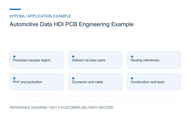
Illustrative engineering application example, not a KFPCBA customer delivery or measured production record. The configurations and calculations below are hypothetical design-review inputs. Project acceptance requires approved drawings and named engineering review.
Let package escape justify the HDI structure
An automotive data or telematics board may combine a processor, memory, communications devices and several external connections. HDI becomes a useful option when package escape or route density cannot be resolved cleanly with the proposed through-hole construction. It should answer a specific interconnect problem, rather than serve as a label for a high-performance board.
This is a board-level engineering example, not a vehicle-qualified T-box or a delivered customer design. An eight-layer, single-build-up concept is one optional study configuration. The actual layer count and via structure remain open until placement, signal references and manufacturing review are complete.
Build a connection map before the via map
Identify the processor package, pin escape, memory interface, Ethernet or other wired link, radio modules and power domains. Define which nets need controlled impedance, timing constraints or a short connector path using their selected device documents. Keep antenna and radio-module requirements separate from the digital interfaces.
Draw the package-to-connector routes on the placement plan. Mark every required layer transition and its reference connection. This reveals whether HDI solves a dense escape, an avoidable placement conflict or both. It also prevents an unnecessary buried-via structure from being specified for nets that could remain on one routing layer.
A hypothetical escape-channel calculation
Assume adjacent pads have 0.80 mm center spacing and each is 0.40 mm wide in the direction being considered. The nominal gap is 0.80 − 0.40 = 0.40 mm. If a proposed trace is 0.10 mm wide with 0.10 mm clearance to each pad, one trace needs 0.10 + 2 × 0.10 = 0.30 mm. Its nominal unused gap is 0.10 mm.
Two such traces need 2 × 0.10 + 3 × 0.10 = 0.50 mm, exceeding the nominal 0.40 mm gap. This simplified drawing check suggests investigating another escape arrangement or layer access. It excludes fabrication tolerances, pad geometry, solder-mask constraints and via lands, so it is not a manufacturability approval or a published process limit.
Specify via spans instead of relying on HDI terminology
Würth Elektronik describes laser microvias as short connections through thin dielectric layers. Its published HDI material is useful background for distinguishing such connections from a through-hole spanning the board. It does not establish a KFPCBA process window.
For the proposed board, make a layer-pair table naming every blind, buried and through connection. Show whether via-in-pad features require filling and capping, and identify any stacked or staggered relationships. Include the proposed lamination sequence for manufacturer review. Terms such as single-build-up or first-order HDI are insufficient if the actual connectivity is not drawn.
Keep the communications channel in the review
The DP83TC812x-Q1 data sheet's signal-routing guidance addresses controlled geometry, trace length and avoiding stubs for its Ethernet implementation. This is a reminder to review the completed channel and the exact PHY revision, rather than assuming that short microvias guarantee link quality.
Check the connector, protection network, reference continuity and host-interface configuration alongside the via arrangement. If changing a via construction also changes the stackup, repeat the affected impedance and channel review. Use the HDI PCB review page to frame the construction discussion, with the proposed rules attached to the actual fabrication package.
Match construction tests to functional tests
| Question | Planned evidence | Record detail |
|---|---|---|
| Are the intended layers connected? | Fabrication netlist test and agreed coupons | Via map, revision and results |
| Does the built structure match the drawing? | Agreed cross-section and fill inspection | Sample locations and measured features |
| Does the communications channel operate? | Defined traffic and interface tests | Cable, PHY settings, firmware and errors |
| Are stresses covered? | Project-specific environmental and assembly plan | Condition sequence and before/after comparisons |
Agreement on the stress plan and acceptance limits is essential. A successful link startup does not by itself establish long-term interconnect behavior, and a coupon result does not establish the complete vehicle network.
Deliver one consistent layer and revision definition
The handoff should contain stackup, drill files separated by span, via definitions, impedance structures, netlist and fabrication notes. Add assembly data, approved component alternatives, the interface constraint list and the tested software configuration. Mark any density-related exception and its approval on the same revision set.
For an initial review, provide the critical package, board envelope and unresolved escape region. Send the available layout through the engineering RFQ to assess the actual interconnect options and required evidence.
HDI data-board questions
Does an eight-layer board automatically require microvias?
No. Package escape and routing can sometimes be resolved using through-holes. Demonstrate the dense region and its constraints before choosing the additional process structure.
Are blind and buried vias interchangeable?
No. They connect different layer spans and may require different fabrication steps. The approved via table must identify each connection explicitly.
Can an Ethernet link test qualify the HDI interconnect?
It is functional evidence for the tested configuration. Construction inspection and the agreed reliability plan address different risks and must remain visible in the acceptance record.
Source material and applicable scope
- Würth Elektronik — HDI Microvia PCBs. Supports the distinction between short laser-drilled microvia interconnects and other board connections; supplier-specific process limits are not adopted. These sources do not establish KFPCBA delivery or capability.
- Texas Instruments — DP83TC812x-Q1 Data Sheet, SNLS654D. Section 9.4.1.1 signal-routing excerpt supports reviewing trace geometry and stubs for this PHY; it is not a complete automotive link qualification. These sources do not establish KFPCBA delivery or capability.