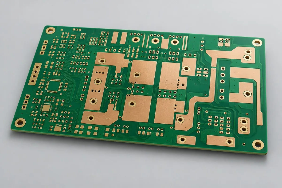
Heavy-copper PCB fabrication: copper weight definitions and current paths
Thick copper PCB manufacturing requires a layer-by-layer description of base copper and finished copper, current paths, and interlayer via arrays. Compare historical 3/3OZ and 4/4OZ constructions with local embedded copper block references, first checking etching, resin fill, and thermal boundaries. Deliver cross-section and net records; copper weight cannot be converted directly into rated current.
Copper weight definition and layer position
Specify base/finished copper, OZ/µm, and corresponding layers in the order documentation and layer stackup. Review pattern, hole, and soldering thermal-mass requirements caused by heavy copper separately. The same maximum copper weight cannot apply to every trace spacing and board thickness combination.
Heavy-copper fabrication: copper weight definitions and current paths
After selecting a product in this category, submit base and finished copper by layer, current-carrying trace widths, via arrays, resin fill, and cooling conditions. Match changes to the reference configuration item by item. Use the same revision for fabrication drawings, inspection locations, and material approval records, and define special verification and reporting scope before quoting.
Back to all PCB products · Manufacturing file knowledge
Material and Process Reference
Consult selected PCB configuration
How do I choose between 3OZ and 4OZ heavy-copper PCBs?
At the same layer count, trace width, and circuit conditions, 4OZ provides a larger copper cross-section than 3OZ while adding fine-trace etching, resin fill, and soldering thermal-mass constraints. Select copper weight using path length, via arrays, allowable voltage drop, and temperature rise. Do not attribute the entire board price difference between six-layer 3OZ and four-layer 4OZ boards to copper weight. Local current or thermal bottlenecks can also be compared with an embedded copper block route.
How do I assess current bottlenecks for full-layer heavy copper versus local embedded copper?
Identify current bottlenecks and thermal paths first, then select 3OZ, 4OZ, or local structures. Thickening only the necessary layers may be more appropriate. Compare options against fabrication trace spacing and lamination conditions.
Thick copper board price and selection common questions
How much do 3OZ and 4OZ heavy-copper PCBs cost? Is thicker copper always better?
A project-specific quotation requires review of the available files, quantity, materials, requested tests, delivery destination, taxes, shipping, and trade terms. This is not a complete finished-product quotation. Base fabrication/sample pricing, special processes, and inspections must not be billed twice. Any formula on this page organizes cost inputs; it is not a quoted rate.View cost items, calculation conditions, and sources.
How to compare thick copper board manufacturer quotes?
Check base and finished copper, trace spacing compensation, via arrays, and lamination together. Thicker copper does not automatically establish system current capacity. Quotes should reflect actual current paths and specified cross-section inspections.
What else should a heavy-copper RFQ specify besides 3OZ?
Specify base and finished copper definitions for each layer, with current paths and via arrays. One copper weight value does not define every layer or establish complete product current capacity.
Does a local bottleneck require increasing the entire board to 4OZ?
First examine narrow traces, corners, terminals, and vias, and compare local widening or embedded copper structures. Thickening the entire board adds etching, resin fill, and soldering constraints. Select based on the complete route.
Should heavy-copper boards and large-terminal soldering be quoted together?
Copper distribution increases thermal mass. Fabrication and assembly must share finished hole, pad, and fastening conditions. Bare PCB manufacturability does not directly establish secondary soldering or load compliance.
Does an accepted copper cross-section guarantee temperature rise performance?
Cross-sections establish construction; temperature rise also depends on actual current, environment, and cooling installation. Separate responsibilities for manufacturing inspection and system load verification. Copper weight does not establish a power guarantee.
Inquire heavy copper board quote: describe the application, existing configuration, and expected quantity so we can discuss bare-board fabrication requirements, inspection, and delivery conditions.
How much do 3OZ and 4OZ heavy-copper PCBs cost? Is thicker copper always better?
Quotes should separately itemize base and finished copper specifications, etching compensation and trace spacing, lamination resin fill and via arrays, and cross-section or specified inspections. Separate initial order setup costs from recurring batch and per-board costs. For the same quantity, also align revisions, delivery configuration, and tax and shipping terms to determine whether price differences reflect configuration or excluded work.
Quotation terms depend on the approved files, quantity, material supply, tests and delivery requirements.
Prepare a structured RFQ or use the short inquiry form.