PCB FABRICATION · ENGINEERING EXAMPLE
Onboard Charger PCB Engineering Example
Engineering Application Example
Review an onboard-charger PCB by separating power-current routing, fast switching loops, isolation boundaries and control measurements before choosing copper weight.
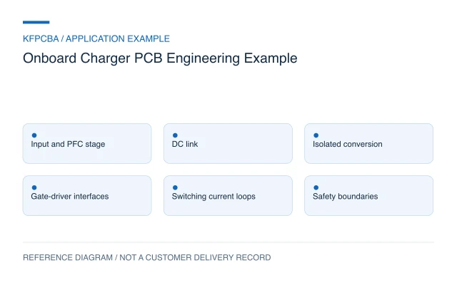
Illustrative engineering application example, not a KFPCBA customer delivery or measured production record. The configurations and calculations below are hypothetical design-review inputs. Project acceptance requires approved drawings and named engineering review.
Use distinct reviews for current flow and isolation
An onboard-charger PCB needs a coordinated electrical, thermal and mechanical definition. Heavy copper can address part of a conduction-loss problem, while switching-loop geometry, insulation boundaries and sensing paths require different decisions. Treating these subjects as one broad power-board requirement hides the reasons for the layout rules.
This is an illustrative board-level planning example. It is not a qualified charger, a construction standard or a procedure for energizing high-voltage hardware. Four layers and heavy outer copper may be considered as design inputs, but neither establishes the completed charger's power, efficiency or insulation performance.
Put the topology and boundaries on one drawing
The system brief should identify the actual conversion topology, input and output conditions, cooling arrangement, switching devices, magnetic components and control interfaces. Draw the boundaries between electrical domains, including auxiliary supplies, drivers, sensing and communication. Record the applicable insulation requirements and the person responsible for approving them.
TI's TIDM-02013 is a published example of a charger architecture combining PFC and an isolated DC/DC stage. It shows why an OBC discussion must identify the stages and interfaces. Its published power and test results apply to TI's reference configuration; they are not specifications for the hypothetical board discussed here.
A hypothetical copper-path loss comparison
Assume an identified conductor path, including its transitions, is provisionally modeled as 4 mΩ. At 12 A, conduction loss is I²R = 12² × 0.004 = 0.576 W. At 20 A with the same resistance, it is 20² × 0.004 = 1.6 W. Increasing current by a factor of 20 ÷ 12 therefore increases this calculated loss by approximately 2.78 times.
The assumed resistance is not a measured PCB value, and these currents are not allowable ratings. Temperature-dependent resistance, current distribution and joint losses are excluded. The calculation helps prioritize a path for analysis and measurement. It does not decide how much copper is sufficient or whether its heat can leave the enclosure.
Review fast loops separately from broad power areas
The UCC21520 data sheet discusses local bypassing and compact gate-current loops for that isolated driver. This supports a separate placement review around a gate driver and its switching devices. Follow the selected device and topology documentation rather than transferring its detailed values to another circuit.
In the board review, distinguish the switching commutation loop, gate-drive loop, low-frequency power path and measurement reference. Check whether a shorter high-current route creates a new coupling problem for the sensing circuit. A large copper area can reduce resistance while still creating undesirable coupling or placing stress on a connector.
Make the insulation drawing govern fabrication details
The design owner must specify the required clearances, creepage paths, slots, material conditions and inspection criteria under the applicable rules. Include component leads, exposed copper, mounting hardware and the final enclosure. Solder mask, coating and a laminate Tg designation must not be used as substitutes for a documented insulation design.
For a heavy-copper proposal, review finished copper by layer, etch allowances, pads, hole construction and the soldering process for power terminals. The thick-copper PCB page provides a starting point for that discussion. Any construction change affecting an electrical boundary needs the system engineer's assessment.
Assign verification evidence by responsibility
| Subject | Planned check | Required record |
|---|---|---|
| Fabricated construction | Netlist, dimensions and agreed cross-section review | Board revision, copper and hole records |
| Power-path heating | Controlled laboratory measurements under the approved plan | Conditions, sensor positions and path temperatures |
| Switching behavior | Qualified review of waveforms and control configuration | Probe method, hardware and software identifiers |
| Electrical separation | Approved insulation inspection and test specification | Method, criteria, results and responsible signoff |
These are evidence categories, not supplied test settings. Bare-board electrical test, assembly inspection, converter performance and system safety assessment answer different questions and should not share a single unexplained pass label.
Keep manufacturing and system acceptance aligned
The controlled package should include fabrication files, stackup, assembly data, domain-boundary drawings, cooling interfaces and approved component alternatives. Include a responsibility table for supplied firmware, magnetic components, mechanical fixtures and each test. State which evidence will accompany the boards and which system checks remain with the integrator.
Begin with the topology, design stage and intended manufacturing scope. Send available files through the quotation request to define a project-specific review; an application name alone is insufficient to confirm a build.
OBC PCB questions
Does doubling copper weight halve total charger loss?
No. Only the resistance of affected paths may change, and joints, switching devices, magnetics and cooling remain part of the loss and temperature problem.
Can isolation be checked from the top copper layer alone?
No. The review includes the complete board construction, component interfaces, hardware and installed geometry under the applicable insulation design.
Can a reference-design efficiency figure be used in a quotation?
It can identify the source design under its stated conditions. It cannot be presented as a result for a different PCB, assembly or KFPCBA project without its own measurements.
Source material and applicable scope
- Texas Instruments — TIDM-02013 Onboard Charger Reference Design. The overview supports distinguishing PFC and isolated DC/DC stages in one published architecture; its specifications and results are not transferred to this example. These sources do not establish KFPCBA delivery or capability.
- Texas Instruments — UCC21520 / UCC21520A Data Sheet, SLUSCJ9F. Section 11 supports a device-specific review of local bypassing and compact gate-current loops; it does not determine system insulation spacing or approval. These sources do not establish KFPCBA delivery or capability.