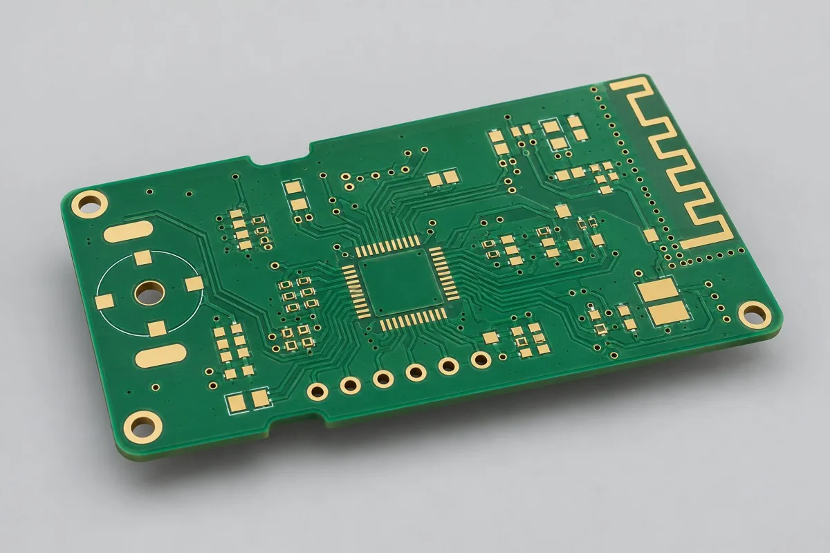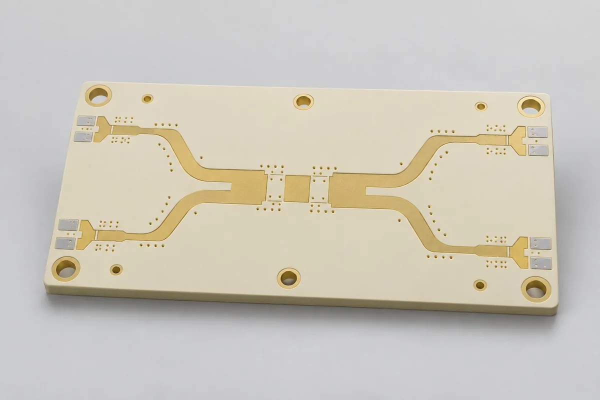
High-Frequency PCB
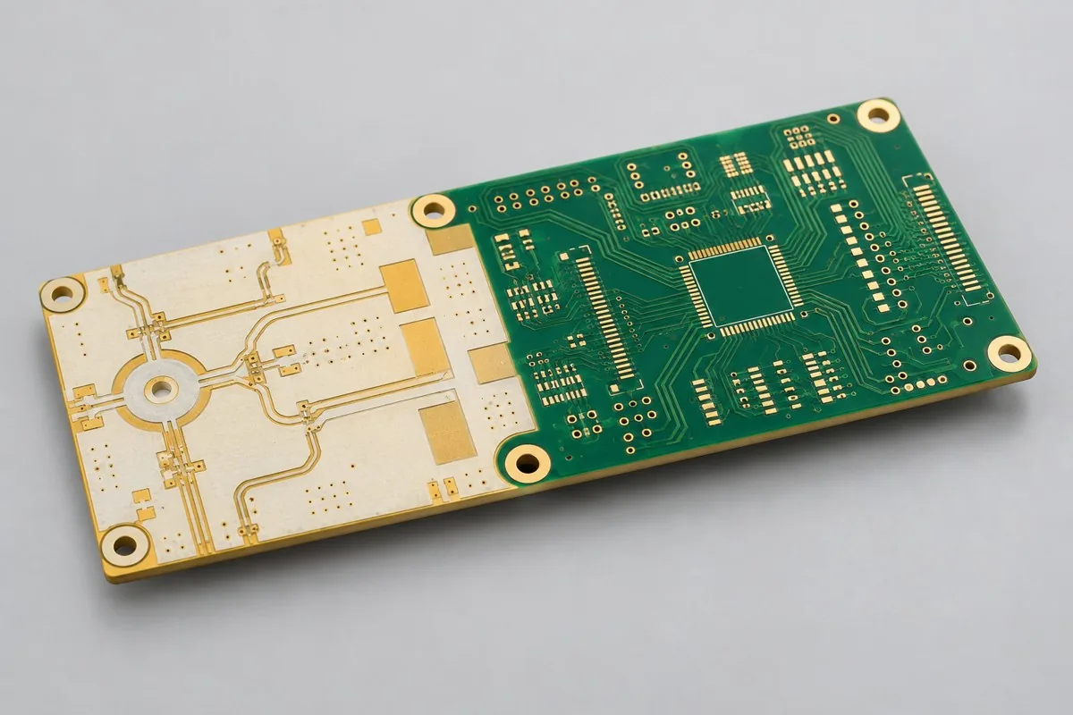
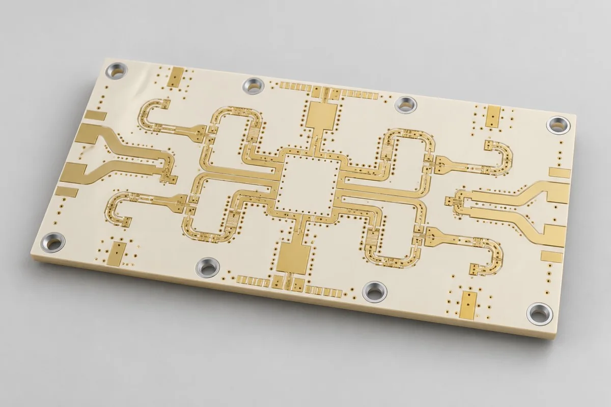
Compare high-frequency PCB materials, dielectric thickness, copper and finishes. Define RF geometry and measurement conditions for fabrication review.
View High-Frequency PCB ConfigurationsQuotes should separately itemize material, area and panel utilization, layer count, hole structures, copper weight and surface finish, engineering setup and electrical testing, specified inspections such as impedance coupons and microsections, and packaging and shipping. Separate initial order setup costs from recurring batch and per-board costs. For the same quantity, also align revisions, delivery configuration, and tax and shipping terms to determine whether price differences reflect configuration or excluded work.
Quotation terms depend on the approved files, quantity, material supply, tests and delivery requirements.
Prepare a structured RFQ or use the short inquiry form.
| Quotation Items | What to verify during comparison |
|---|---|
| Panel material, area, and panelization utilization rate | Individual board dimensions and panel layout determine material utilization. For panel pricing, also confirm the number of usable individual boards delivered. |
| Layer count, hole structures, copper weight, and surface finish | Blind and buried vias, heavy copper, and different surface finishes add different fabrication steps. Costs should correspond to the approved drill table and stackup. |
| Engineering Preparation and Electrical Testing | Engineering setup is a batch investment, while electrical testing is an agreed board inspection. List initial and repeat order costs separately. |
| Specified inspections such as impedance coupons and microsections, plus packaging and shipping | Test coupons occupy panel space, and microsections require a sampling definition. Compare reports, packaging, and freight for the agreed quantity and delivery method. |
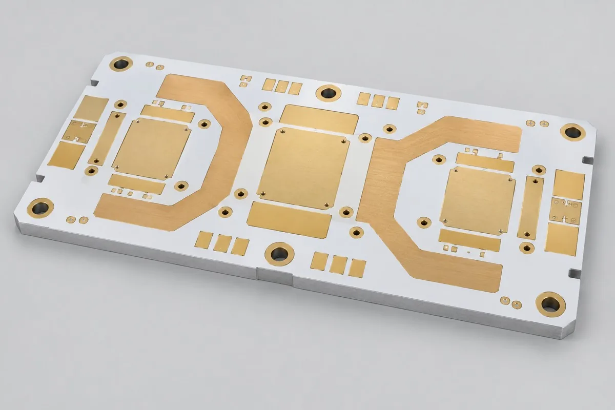
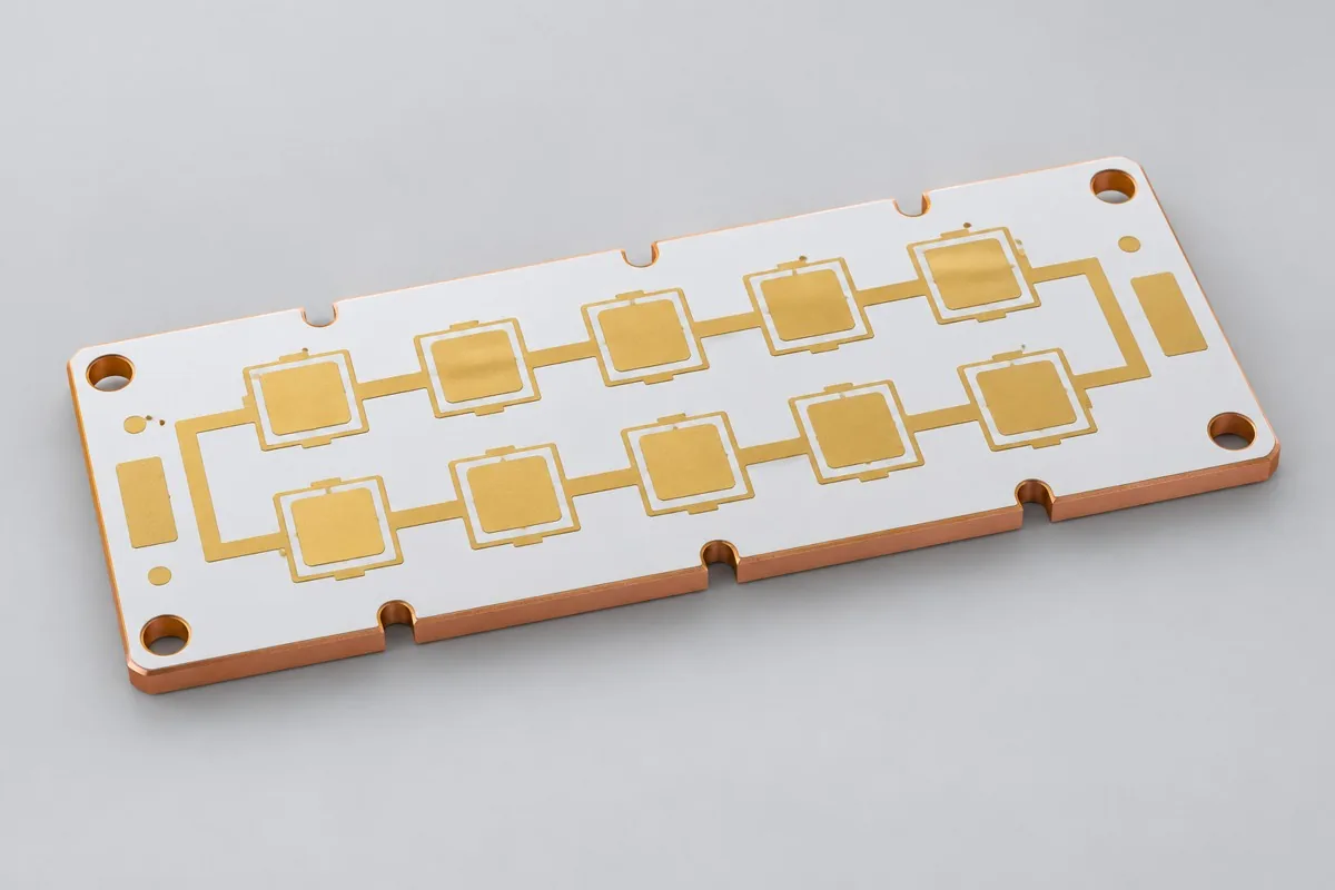
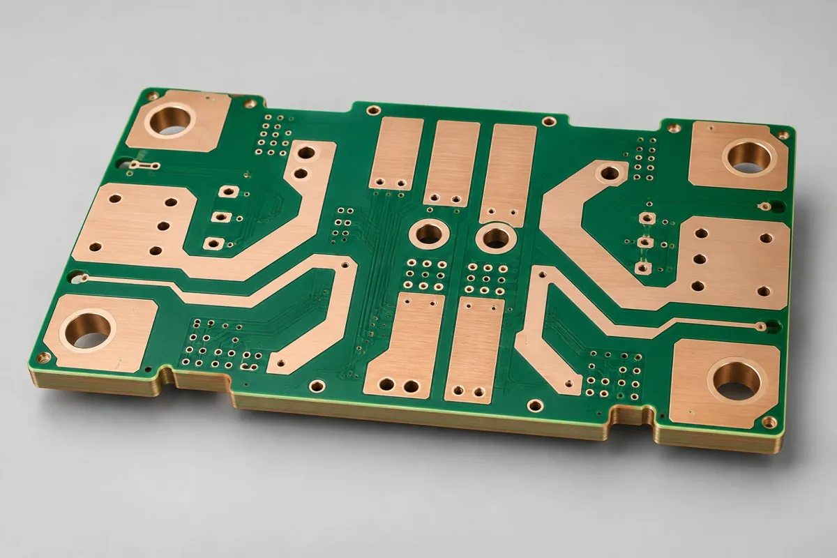
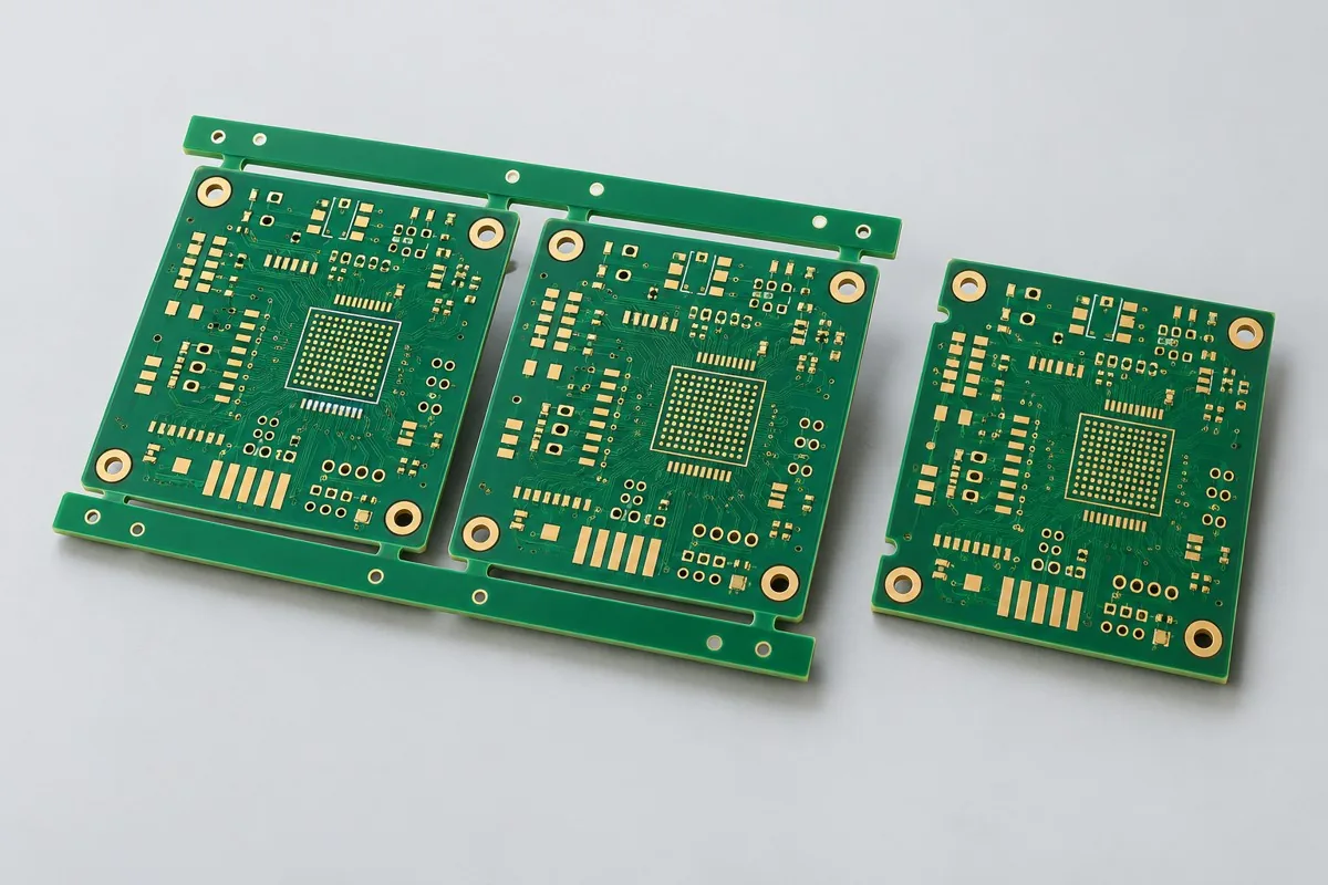
Standard FR4 suits conventional control and interfaces. High-frequency materials serve RF paths constrained by loss and transmission geometry. Heavy copper and metal-core constructions address current carrying and thermal paths, respectively. Different board types cannot be ranked by area-based pricing alone.
First establish the signal, power, or mechanical interconnect task, then select layer count, materials, and processes. Prototypes focus on verification; production comparisons use a fixed revision to compare delivered quantities and allocation of one-time setup costs.
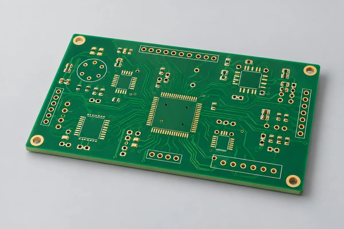
PCB fabrication delivers bare boards without components, with materials and construction selected for development prototypes or production requirements. First confirm Gerber files, drills, outline, stackup, copper weight, and quantity. For custom PCBs, choose processes based on specific high-frequency, HDI, heavy-copper, or metal-core requirements. Prototype requirements can be addressed in the PCB prototyping category.
| requirement | Key Comparison Points | Product Entry |
|---|---|---|
| RF/Microwave/Antenna | Material Dk/Df, RF layer location, copper foil/surface finish, and port/feed structure | 6 high-frequency configurations · 4 Rogers-material configurations · 3 hybrid-material configurations |
| Interface, computing and control | Reference planes, layer count, microvia fanout, through-hole stubs, and measurable target nets | Impedance Interface Product · HDI Product · Multi-Layer Products |
| Power/thermal/mechanical connection | Copper cross-section/via arrays, insulating thermal path, rigid-flex interfaces, or contact plating | Heavy Copper/Embedded Copper Block · Metal Substrates · Rigid-flex connections · Gold fingers |
Label historical configurations separately from engineering references. Materials, total thickness, dielectric thickness, hole diameters, and surface finish are confirmed against approved fabrication drawings. Review parameters together; separate extreme values cannot be combined into a manufacturing commitment for one board.
Gerber manufacturing documents · HDI Lamination Knowledge · Prototype Material Preparation Knowledge · PCB manufacturing capability data · Material Review · Stackup Review
PCB Bare Board Quotation: submit the product ID, application, quantity, Gerber files, drills, outline, and stackup. Specify materials, copper weight, and specifications to adjust so a bare PCB quote revision can be established.
A project-specific quotation requires review of the available files, quantity, materials, requested tests, delivery destination, taxes, shipping, and trade terms. Add specified materials, processes, and inspections not yet included to the total cost. Standard board references do not cover every configuration of this product. Any formula on this page organizes cost inputs; it is not a quoted rate.View cost items, calculation conditions, and sources.
Require PCB quotes to reference the actual stackup, material grade, and finished copper weight. Then check whether electrical testing, impedance reports, microsections, and shipping are included. Compare equal individual board or panel quantities to distinguish material price differences from inspection scope differences.
Bare PCBs exclude BOM components, assembly, programming, and functional test support. For PCB assembly, provide the BOM and pick-and-place file separately and price the two delivery items separately.
Retain the original specified requirements, list candidate grades, actual stackup, and affected nets, and obtain approval from the authorized project party for recalculation and verification. An unapproved substitute price cannot be treated as the lowest price under equivalent conditions.
Specify boards per panel, complete panel or depanelized delivery, and acceptance rules for defective positions. Match costs to accepted delivered quantities; internal production panel layouts do not automatically define purchasing counts.
Continuity, specified transmission structures, and cross-sectional geometry are different inspection targets. Define scope, board/coupon IDs, and reports according to this board's risks. One pass result cannot replace all three record types.
Confirm individually whether engineering file processing, dedicated tooling, and special verification are separately charged. Calculate materials, fabrication, electrical testing, and packaging for the batch scope. List reusable approved files and tooling for repeat orders separately from manufacturing and inspection that must still be performed; do not assume all preparation remains free forever.
First freeze actual materials, stackup, holes, and surface finish, and close pilot-run changes. Then requote for production panel layout, accepted delivery quantity, and inspection scope. Items inadequately verified in prototyping still require confirmation; do not simply scale the original order by quantity.
List changes to board drawings, stackup, materials, and acceptance criteria, and determine individually whether CAM, tooling, impedance structures, and reports must be redone. Discuss reuse of unchanged, usable support items; every batch must still include fabrication and inspection work.
Inquire PCB manufacturing quotation: describe the application, existing configuration, and expected quantity so we can discuss bare-board fabrication requirements, inspection, and delivery conditions.
Quality and acceptance · Production equipment · Engineering RFQ with PCB files
Browse by product type, then compare configuration details, process tradeoffs, and verification requirements.
Compare high-frequency PCB materials, dielectric thickness, copper and finishes. Define RF geometry and measurement conditions for fabrication review.
View High-Frequency PCB ConfigurationsReview hybrid PCB stackups combining different material systems. Check lamination compatibility, thickness, via structures and impedance requirements.
View Hybrid-Material PCB ConfigurationsCompare Rogers PCB material grades and construction options. Specify the exact laminate, copper, dielectric thickness and RF acceptance requirements.
View Rogers PCB ConfigurationsSelect high-Tg PCB materials using thermal properties, assembly exposure and reliability requirements. Review the material grade with the intended stackup.
View High-Tg PCB ConfigurationsSpecify controlled-impedance PCBs with layer geometry, materials and target nets. Agree fabrication tolerances, test coupons and measurement conditions.
View Impedance-Controlled PCB ConfigurationsSelect FR-4 PCB construction by electrical, thermal and mechanical needs. Compare laminate grades, thickness, copper and fabrication requirements.
View FR-4 PCB ConfigurationsPrepare PCBs for lead-free assembly with suitable laminate, finish and thermal requirements. Verify material declarations for the actual order scope.
View Lead-Free PCB Selection ConfigurationsCompare HDI buildup routes, microvia layer pairs and fine-pitch breakout needs. Review stackup, via reliability and fabrication documentation together.
View HDI PCB ConfigurationsDefine multilayer PCB construction through layer order, planes, copper balance and via spans. Align stackup, impedance and electrical-test requirements.
View Multilayer PCB ConfigurationsReview RF PCB fabrication by signal path, grounding, connectors and measurement references. Specify material and geometry for the operating band.
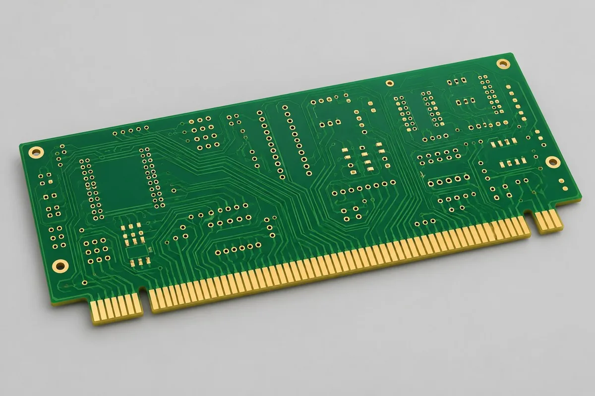
View RF PCB ConfigurationsSpecify PCB edge contacts by connector geometry, plating area, thickness and bevel. Separate mating-contact requirements from solderable surface finishes.
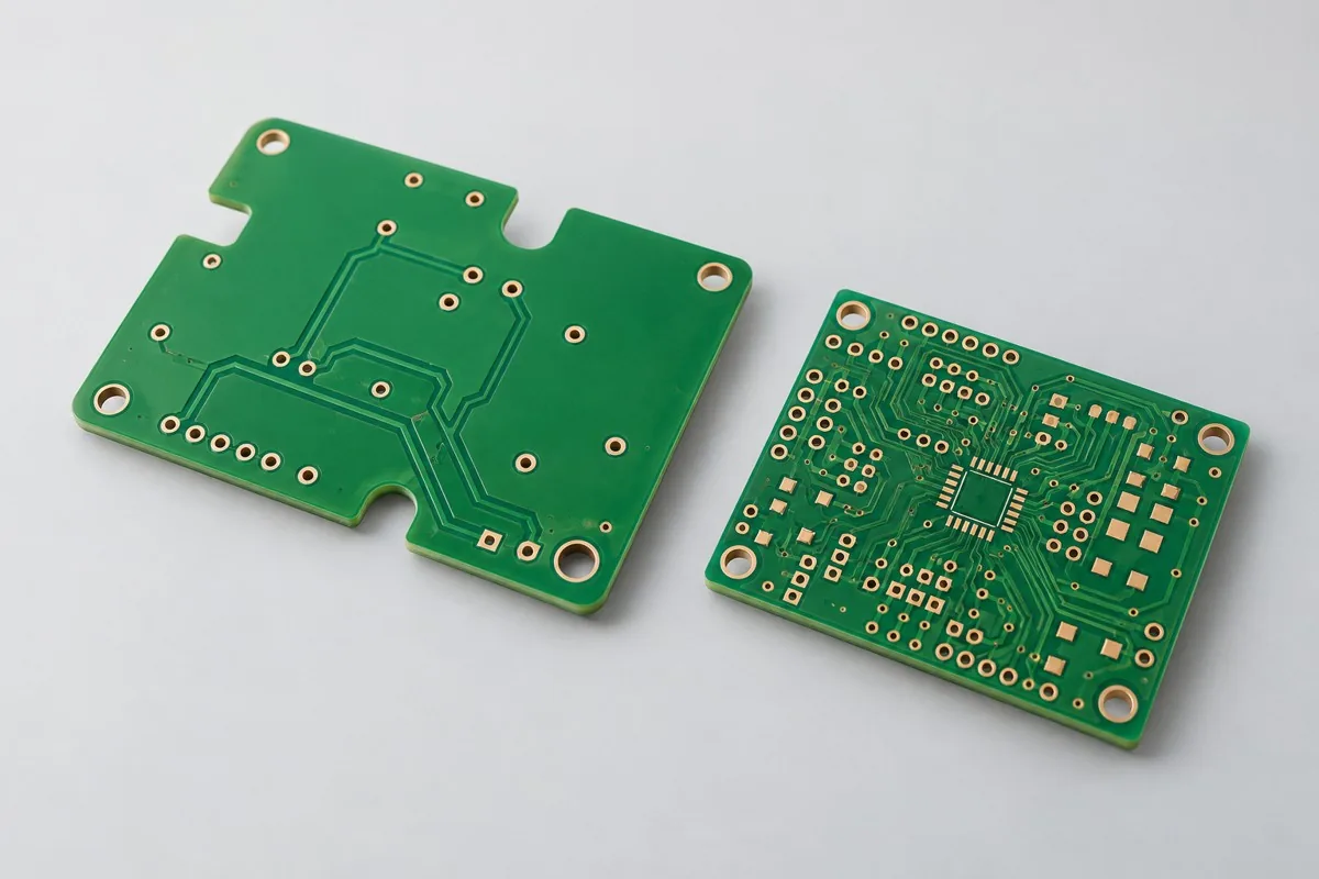
View Gold Finger PCB ConfigurationsCompare single- and double-sided PCBs by routing, plated holes and assembly needs. Prepare fabrication files, materials, finish and test requirements.
View Single- and Double-Sided PCB ConfigurationsCompare rigid-flex and semi-flex PCB constructions for static forming and interconnection. Define bend areas, materials, reinforcement and mechanical limits.
View Rigid-Flex and Semi-Flex PCB ConfigurationsCompare aluminum-core PCBs by dielectric insulation, thermal path and mounting needs. Review material, copper and fabrication requirements together.
Select metal-core PCB construction using thermal, electrical and mechanical constraints. Define insulation, copper, mounting and acceptance requirements.
View Metal-Core PCB ConfigurationsReview heavy-copper PCB construction for current paths, heat spreading and fabrication constraints. Specify copper by layer and validate the complete design.
View Thick Copper PCB ConfigurationsPrepare a PCB prototype build with released files, material choices and validation priorities. Plan the changes needed before a repeat production order.
View PCB Prototyping Configurations
Tell us the product use and which files are available. We can define the next engineering step even when the data package is not complete.