
Prototype Phase
Validate sleep/wakeup, data upload, or positioning paths with the battery, enclosure, and antenna; record operating and transmit currents.
From sensor nodes to wireless gateways, check the interaction of low-power design, RF, and enclosure, along with programming, device IDs, networking, and data-acquisition tests.
Consult IoT consigned PCB assembly →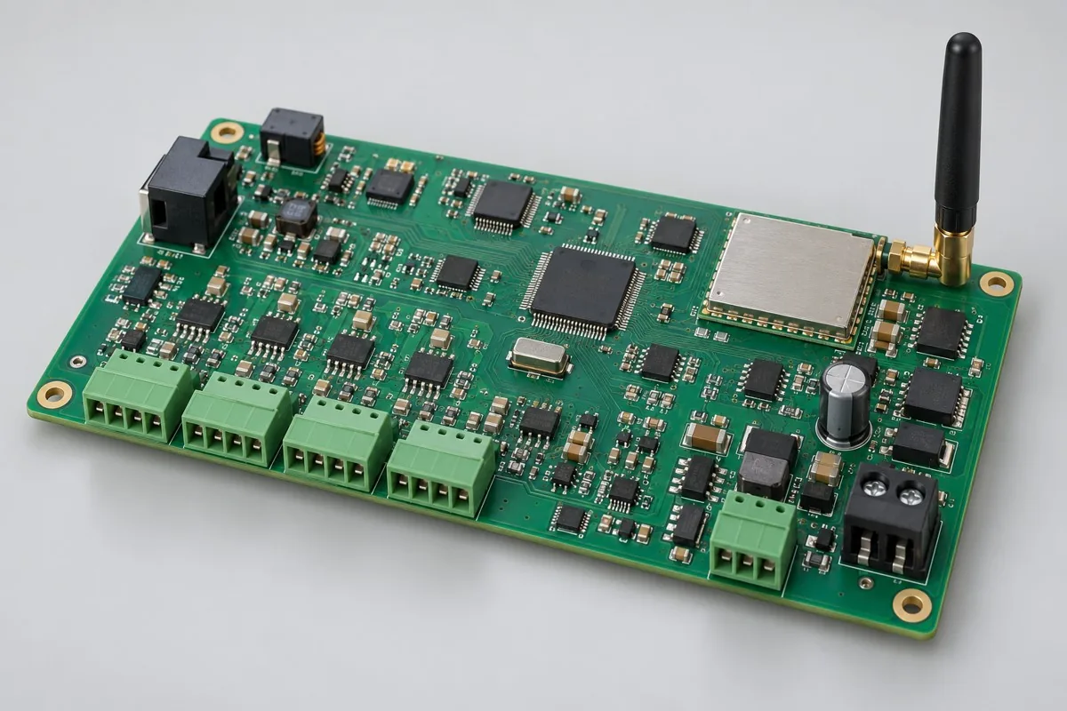
| Project Direction | PCB Manufacturing and Layout Focus | PCBA assembly and testing highlights |
|---|---|---|
| Battery sensing node | Leakage paths, antenna clearance, sensor positions, and battery connections | Standby/transmit current, wakeup, sampling, and low-voltage behavior |
| Wireless data gateway | RF/digital partitioning, interface protection, power, and network connectors | Serial/Ethernet/wireless links, reconnection after link loss, and data upload |
| Positioning and tracking module | GNSS antennas and RF feedlines, charging protection, and mechanical clearance | Positioning data, communication, charging/discharging, unique IDs, and firmware verification |
| Review Items | What specific inputs are provided | How to confirm results |
|---|---|---|
| Low Power | Operating/sleep modes, voltage, current limits, and measurement bandwidth | Select test equipment and sampling methods that measure sleep current and transmit peaks |
| RF System | Frequency bands, module revisions, antenna types, and enclosure materials | Board-level RF testing and complete-unit antenna validation use different fixtures and criteria |
| Production Identity | Responsibility for serial numbers, communication addresses, key programming, and backend binding | Agree on permissions, duplicate-ID blocking, programming readback, and log redaction |
Validate sleep/wakeup, data upload, or positioning paths with the battery, enclosure, and antenna; record operating and transmit currents.
Freeze programming, device-ID, and key-authorization procedures, and validate duplicate-identity blocking, programming readback, and network-outage recovery.
Perform programming and networking tests according to configuration and permissions, retaining redacted logs, revisions, and batches; backend binding and key ownership follow project responsibilities.
For IoT projects, in addition to Gerber, drill files, BOM, pick-and-place files/CPL, and assembly drawings, include operating environment, actual interfaces/loads, enclosure and harness drawings, target quantity, and the test limits above. If commissioning programming or calibration, add software revision, checksum, fixture wiring, and programming permissions.
Board-level RF, complete-unit antennas, and backend services use different interfaces and criteria; define authorization to receive device identities and keys.
View specific fabrication products by board-level task, or arrange a joint PCB fabrication and assembly review with complete information.
Engineering reference | QFN and SON assembly: thermal pads, printing, and solder joint verification: QFN/SON pad, stencil, and measured thermal process methods; not company capabilities.
Engineering reference | Packaging PCB fabrication files: units, layer order, and engineering notes: methods for PCB fabrication, hole layer spans, and file semantics.
| Work area | Inputs or responsibility | Expected output |
|---|---|---|
| Power | Operating states, sleep and wake behavior | Define measurement conditions and configuration |
| RF and enclosure | Antenna, mechanics and intended operating environment | Identify validation and regulatory responsibilities |
| Identity | Device identifier, firmware and credential provisioning | Agree access, logging and handoff responsibilities |
| Recovery | Connection loss, power interruption and update failure | Define the required behavior and test evidence |
Use the electronics-development scope to prepare the discussion. Unknown inputs should be listed as open questions; they do not authorize substitutions, omitted tests or unrecorded design changes.

Tell us the product use and which files are available. We can define the next engineering step even when the data package is not complete.