PCB FABRICATION · ENGINEERING EXAMPLE
AR/VR Head-Unit PCB Engineering Example
Engineering Application Example
Plan an AR/VR compute and display board around actual interfaces, mechanical space, heat sources and verification evidence before choosing layer count.
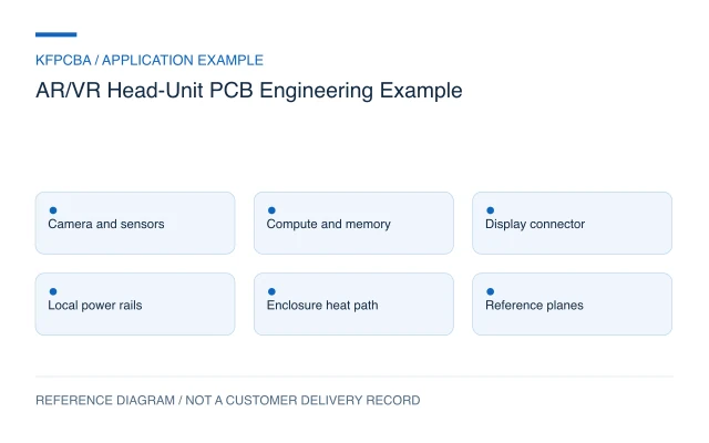
Illustrative engineering application example, not a KFPCBA customer delivery or measured production record. The configurations and calculations below are hypothetical design-review inputs. Project acceptance requires approved drawings and named engineering review.
Start with the display and sensor paths
An AR/VR head-unit PCB should be planned around the complete path from image capture and processing to the display connector. A high layer count can provide routing space, but it cannot establish display stability, tracking performance, thermal comfort or electromagnetic compatibility. First identify the processor, memory, display interfaces, sensor buses and power states, then decide whether the placement can support their electrical and mechanical requirements.
This example concerns a compute and display board. It does not establish optical alignment, motion-to-photon latency, vehicle suitability or a qualified end product. A twelve-layer stackup is only one possible study input; another design may need fewer layers, a different interconnect structure or a separate display board.
Freeze the interfaces before allocating layers
Create an interface table showing each transmitter and receiver, lane count, data format, connector, cable and relevant device revision. List display resolution and refresh modes separately from camera capture modes. Include boot, standby, update and maximum processing states so that power distribution is reviewed across the operating sequence.
Use the enclosure model to reserve lens or optical-module clearance, mounting datums, connector insertion space and the heat-spreader contact area. Give antenna keepouts and flex exits their own boundaries. Otherwise, an electrically convenient processor location may force a cable fold or heat path that the assembled product cannot accommodate.
A hypothetical display-payload calculation
Assume two displays, each with 1600 × 1600 active pixels, 90 frames per second and 24 bits per pixel. The active-image payload is 2 × 1600 × 1600 × 90 × 24 = 11,059,200,000 bits per second, or approximately 11.06 Gbit/s. This is arithmetic for the stated hypothetical mode, not a supported board or interface rate.
The number excludes blanking, protocol encoding, packet overhead and implementation margin. Compression and link arrangements can change the required physical transmission rate. Use the actual display timing and transmitter documentation to convert this payload into a lane configuration. It is a useful early rejection check: a preferred connector or routing corridor should not be selected before the link budget is known.
Review return paths before adding more routing layers
TI's High-Speed Interface Layout Guidelines discusses continuous reference planes, pair symmetry and via discontinuities. These are relevant review subjects for a display or camera channel; the selected interface devices still determine the detailed constraints. Avoid applying a generic trace-length rule to every bus.
For this review, mark each high-speed route and its reference plane together. Flag plane changes, mounting-hole voids, connector breakouts and long unused via sections. Separately map switching-power areas, clock sources and heat-spreader attachments. The design decision is whether placement or layer assignment can remove a difficult transition before extra routing layers are added.
Turn the stackup proposal into a fabrication definition
Compare a through-hole multilayer concept with an HDI alternative only after checking package escape and routing congestion. Specify the proposed material family, dielectric thicknesses, copper by layer and controlled-impedance structures as review inputs. A Tg shorthand does not describe high-frequency loss, thermal expansion or the completed channel.
Ask for a fabrication review of the actual drill structure, impedance coupons, board outline and flatness requirements. Agree how approved substitutions will be assessed. Use the PCB fabrication process page to frame the manufacturing discussion, without treating the page as confirmation of this particular stackup.
Separate board checks from headset performance
| Question | Method to agree | Evidence to retain |
|---|---|---|
| Does the board match its design? | Netlist test, dimensions and agreed impedance coupons | Fabrication revision and numerical records |
| Does the display path operate? | Selected modes with actual display and cable | Link settings, errors and repeatable image observations |
| Do simultaneous tasks disturb it? | Display, cameras and processing active together | Supply waveforms, temperatures and error logs |
| Does final assembly change behavior? | Compare open board with installed enclosure | Heat-spreader, cable and enclosure configuration |
Set acceptance limits in the approved system plan. A continuity report cannot stand in for image quality or tracking tests. If a fault appears only after assembly, preserve the cable position and mounting state before changing the PCB.
Hand over a reproducible configuration
The review package should contain fabrication files, stackup, netlist, assembly drawings, BOM alternatives and interface constraints. Add the connector and cable revisions, thermal-contact drawing, firmware image identifier and test-mode instructions. A display fault is difficult to reproduce when the tested cable or software version is unknown.
For an initial discussion, state the interfaces, enclosure envelope and present design stage. Submit available files through the engineering RFQ; the next step is a project-specific assessment of the missing inputs and proposed verification scope.
AR/VR PCB questions
Does twelve layers guarantee enough display bandwidth?
No. Layer count does not specify the transmitter, connector, material losses or completed channel. Check the exact mode and physical path before selecting the layer count.
Can the heat spreader be positioned after routing?
Reserve its mounting and contact geometry during placement. Later relocation may change component clearance, board loading and cable routing, so electrical and mechanical reviews must remain connected.
Should every sensor trace be length matched to the displays?
No. Build timing groups from each interface specification. Unnecessary matching consumes routing space and may create additional bends without addressing the actual timing relationship.
Source material and applicable scope
- Texas Instruments — High-Speed Interface Layout Guidelines, SPRAAR7J. Sections 2.4 and 3 support reviewing reference continuity, differential routing and transition discontinuities; they do not define an AR/VR system performance result. These sources do not establish KFPCBA delivery or capability.