Engineering Selection Reference
Four-layer RO4350B: specialty-dielectric RF board fabrication review
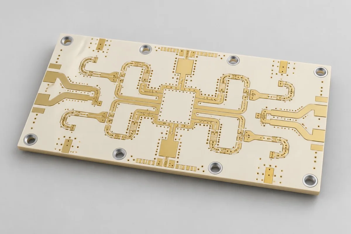
Four-layer specialty-dielectric RF fabrication requires review against current drawings. For commissioned four-layer RO4350B specialty-dielectric bare boards, approve cores, RO4450F bonding layers, and RF via layer pairs under one revision. All-specialty construction still involves pressed dielectric-thickness and transition-via risks. Deliver material layer tables, microsections, and agreed layer-specific coupons; specifications are an Engineering Reference Configuration.
For four-layer RO4350B boards, first define bare-board prototyping or production scope. Please provide Gerber data, drill files, board outline, and layer stackup, materials/processes, quantity, and manufacturing acceptance requirements. Four all-specialty-dielectric layers differ from FR4 hybrid construction; pressed bonding-sheet dielectric also enters the model
Four-layer specialty-dielectric RF review starts with RO4350B cores and RO4450F bonding layers; quotations also need layer-by-layer materials and RF via layer pairs. Subsequent specification and manufacturing-input tables link design targets to inspection methods.
Why choose this specialty-dielectric multilayer structure
When RF paths must enter internal transmission, shielding, or component interconnections rather than remain outside, consider a four-layer RO4350B+RO4450F specialty-dielectric board. Unlike FR4 hybrid construction, it places every interlayer electromagnetic environment within a specialty-material system, while still requiring separate bonding-layer modeling.
What determines the price of an all-specialty-dielectric four-layer RO4350B PCB?
Costs include RO4350B cores, RO4450F bonding sheets, inner traces, lamination, through holes, and layer-specific inspections. Compare with FR4 hybrids by identifying every RF layer and ground reference, not simply four-layer Rogers. Quote internal shielded transmission lines, microsections, and layer-transition VNA deliverables separately; ordinary four-layer electrical-test scope cannot replace specialized RF verification.
Quotation terms depend on the approved files, quantity, material supply, tests and delivery requirements.
Prepare a structured RFQ or use the short inquiry form.
Enter the following items in one itemized quotation: specify cost units and tax/shipping basis, with separate columns for first orders and same-revision repeat orders. The table is a procurement breakdown method, not a ready-made price list; reference specifications require approval against current fabrication drawings.
| Quotation items and pricing boundaries | Actual inputs requiring alignment for this model | Repurchase of same version and change boundaries |
|---|---|---|
| Materials/fabrication, quoted per batch or accepted board | RO4350B cores+RO4450F bonding sheets; 4 layers; outer base copper 18µm/finished 35µm; inner copper target 35µm | Recurs on repeat orders; material, layer-order, or copper-weight changes require requotation |
| Holes and forming, per approved hole table | Ø0.25mm through holes; paired RF-transition return vias | Reorders follow the same revision; review operations before changing specialty-dielectric layer sequences |
| Surface finish/packaging, noting areas and batches | Silver immersion; do not cover solder mask on critical transmission lines | Incurred by actual batch; confirm packaging, storage conditions, and surface-finish substitutions separately |
| Engineering/tooling preparation, identifying one-time or per-batch charges | Specialty-dielectric layer sequence: specify RO4350B cores, RO4450F bonding sheets, and signal-layer roles by layer; four-layer Rogers alone is insufficient. | Verify file revisions, ownership, and storage condition before reusing old tooling; do not assume reuse is free |
| Structural/special inspections, identifying coupons, hole groups, or samples | Retain approved material BOM, pressed-thickness targets, and impedance-coupon layer mappings. Release hole tables and electrical-test netlists under the same revision. | List initial prototype validation and per-batch sampling separately; quote per-board requirements separately rather than assuming everything is completed once |
| Delivery scope, listing reports and pass quantity | Four-layer specialty-dielectric bare PCB, material layer table/RO4450F lots, stackup microsection records, and layer-specific impedance coupons; RF layer-transition structures may accompany the board. | Retain revision links and batch records on repeat orders; list component assembly, firmware, and complete-unit testing separately |
How do all-RO4350B four-layer boards differ from RO4350B/FR4 hybrids?
All-specialty dielectrics suit RF paths entering inner layers or requiring internally shielded transmission. FR4 hybrids suit structures where specialty dielectric serves designated RF layers and other layers serve control. Actual RF layer pairs determine whether the all-specialty system is worthwhile; where digital regions lack equivalent dielectric needs, compare material investment with functional benefit.
| Comparison Dimension | Four-layer RO4350B PCB fabrication | Six-layer RO4350B hybrid PCB |
|---|---|---|
| Material and Grade | RO4350B cores+RO4450F bonding sheets | RO4350B RF core+370HR FR4 digital region |
| Layer Count and Structure | 4 Layer | 6 Layer |
| Hole Structure and Dimensions | Ø0.25mm through holes; paired RF-transition return vias | Ø0.30mm through holes; RF L1 does not cross reference-plane gaps |
| Application | Multilayer RF modules; microwave circuits with internal shielding | MCU-controlled RF instruments; RF digital acquisition interfaces |
How does RO4450F thickness affect four-layer RF board selection?
Pressed bonding thickness depends on copper density and lamination and differs from core thickness. Inner traces within bonding dielectric require its corresponding properties and pressed thickness in calculations. Specify cores, bonding sheets, and copper density together; update models from first-article microsections rather than applying core Dk to every layer.
| Decision Sequence | This Model Input | Generated Auditable Output |
|---|---|---|
| 1 define usage and boundaries first | Specify RO4350B cores, RO4450F bonding sheets, and signal-layer roles by layer; four-layer Rogers alone is insufficient. | Retain approved material BOM, pressed-thickness targets, and impedance-coupon layer mappings. |
| 2 fixed conditions affecting structure | Mark layer pairs for RF ground vias and functional through holes; determine whether they share diameters and fabrication steps. | Release hole tables and electrical-test netlists under the same revision. |
| 3 Align Networks with Manufacturing Targets | Outer-layer 50Ω; field solving+TDR for internal shielded transmission lines | Provide target nets, layer pairs, and verification scope; review with Ø0.25mm through holes and paired RF-transition return vias |
| 4 then verify quotation and release | RO4350B cores+RO4450F bonding sheets; 1.02mm reference target; immersion silver; no solder mask over critical transmission lines | Request quotations using material/pattern/inspection lists at the same revision; list unapproved substitutions as separate alternatives rather than including them in the baseline quotation |
Specialized dielectric multilayer board manufacturing specifications
| Specification Items | Clarify Configuration/Target |
|---|---|
| Material and Grade | RO4350B cores+RO4450F bonding sheets |
| Layer Count and Structure | 4 Layer |
| Total Board Thickness | 1.02mm reference target |
| Dielectric thickness and interlayer relationship | Top/bottom RO4350B each 0.254mm; RO4450F pressed target approximately 0.37mm; recheck total thickness against copper weight |
| Base Copper and Finished Copper | Outer base copper 18µm/finished 35µm; inner copper target 35µm |
| Hole Structure and Dimensions | Ø0.25mm through holes; paired RF-transition return vias |
| Trace Width and Spacing | 0.125/0.125mm reference design |
| Impedance Target and Measurement Methods | Outer-layer 50Ω; field solving+TDR for internal shielded transmission lines |
| Surface Finish | Silver immersion; do not cover solder mask on critical transmission lines |
| Original Material Specifications | RO4350B: process Dk 3.48±0.05, design Dk 3.66; Df 0.0037 (10GHz, manufacturer typical values) |
| Application | Multilayer RF modules; microwave circuits with internal shielding |
| Deliverables | Four-layer specialty-dielectric bare PCB, material layer table/RO4450F lots, stackup microsection records, and layer-specific impedance coupons; RF layer-transition structures may accompany the board. |
Layer stackup and hole structure for dedicated dielectric multi-layer board
The following shows functional layer order/material structure for this reference configuration, not a production stackup drawing; do not infer thickness from graphic proportions. Match copper-layer numbering to via layer pairs item by item in approved fabrication files.
| Top to Bottom | Layer Responsibilities/Structure |
|---|---|
| L1 | External RF Signal |
| L2 | Reference Ground |
| L3 | Internal RF Signal |
| L4 | Reference Ground |
Hole structure: Ø0.25mm through holes; paired RF-transition return vias
RO4350B dielectric and loss models
Use corresponding material parameters separately for RO4350B cores and RO4450F bonding layers; determine pressed RO4450F dielectric thickness from copper density and lamination results. Match each RF layer to actual reference ground, copper weight, and solder-mask windows before solving transmission geometry; core Dk cannot replace bonding-layer Dk.
All-specialty-material costs versus pressed dielectric thickness
All-specialty materials increase material costs but do not automatically eliminate reflections at outer-to-inner transitions. RO4450F pressed thickness varies with layer count, copper density, and lamination; 0.37mm here is only a design target. Do not substitute supplied unpressed thickness into impedance calculations.
RF layer sequence, antipads, and ground-return vias: manufacturing checks
Freeze core, bonding-sheet, and copper-foil revisions together; RF layers must not be swapped for CAM convenience. Check antipads and ground-return vias at transitions; inner-layer AOI/registration checks concern critical geometry hidden after fabrication.
Inner/outer TDR and layer-transition VNA: acceptance items
Provide separate coupons for outer microstrip and inner transmission lines, using first-article microsections to verify pressed dielectric thickness. VNA verification includes at least one critical layer transition. Define parameters for the specific RF circuit; bare-board electrical testing covers only net continuity and shorts.
Specialized dielectric multilayer board delivery scope
Applications: multilayer RF modules; microwave circuits with internal shielding.
Four-layer specialty-dielectric bare PCB, material layer table/RO4450F lots, stackup microsection records, and layer-specific impedance coupons; RF layer-transition structures may accompany the board.
Layer-by-layer material table and RF via layer pairs: quotation inputs
Submit layer-by-layer materials and RF via layer pairs, converting tabled targets into inspectable drawings. The following inputs separately define artwork, material, or structural inspection scope; freeze quotation revisions with approved drawings.
| Inputs required to be completed for this product | Engineering Decisions Affected | Records/delivery as agreed in the order |
|---|---|---|
| Dedicated Dielectric Stackup | Specify RO4350B cores, RO4450F bonding sheets, and signal-layer roles by layer; four-layer Rogers alone is insufficient. | Retain approved material BOM, pressed-thickness targets, and impedance-coupon layer mappings. |
| Ground Connection Hole | Mark layer pairs for RF ground vias and functional through holes; determine whether they share diameters and fabrication steps. | Release hole tables and electrical-test netlists under the same revision. |
Four-layer RO4350B PCB fabrication: pricing, selection, and procurement FAQ
What determines the price of an all-specialty-dielectric four-layer RO4350B PCB?
A project-specific quotation requires review of the available files, quantity, materials, requested tests, delivery destination, taxes, shipping, and trade terms. Add any specified processes and tests not yet included to the batch budget; a quotation for this configuration does not apply to other materials or layer sequences. Any formula on this page organizes cost inputs; it is not a quoted rate.View cost items, calculation conditions, and sources.
How do all-RO4350B four-layer boards differ from RO4350B/FR4 hybrids?
When RF enters internal layers, all-specialty dielectrics provide the corresponding interlayer electromagnetic environment; compare FR4 hybrids when specialty dielectric serves one RF side and other layers handle control. Actual RF layer pairs determine its value; material names do not establish identical dielectric needs for all digital layers. View Specific Comparison Basis
How does RO4450F thickness affect four-layer RF board selection?
RO4450F pressed thickness varies with copper density and lamination; inner traces need corresponding bonding-material parameters and actual dielectric thickness. RO4350B core Dk cannot represent the bonding layer. Update models from first-article microsections rather than treating supplied unpressed thickness as finished-board spacing. View Specific Comparison Basis
Can a four-layer Rogers board become double-sided to reduce cost?
Compare this only when RF and control paths can be rearranged onto one side while retaining continuous ground on the other. If internal RF or shielding still needs layer space, deleting layers changes function; reroute and verify first.
Does a four-layer RF quotation include RO4450F lot documentation?
Include core and bonding-sheet lot records in material deliverables, mapped separately to the approved stackup. Recording only RO4350B grade does not identify actual interlayer dielectric or procurement revision.
If inner and outer traces are both 50Ω, does the RF layer transition pass?
Acceptable trace impedance does not imply a reflection-free transition. Via pads, antipads, and return vias jointly affect it; check port response using at least the specified layer-transition test structure.
How can I determine which layers to retain in a four-layer all-specialty-dielectric board?
Mark internal RF paths and reference grounds on routing drawings and list control-only layers separately. Retain specialty materials where internal shielded transmission is required; develop a hybrid alternative only if RF stays outside. Preserve the original frequency band and port testing in comparisons rather than replacing RO4450F with the FR4 label directly.
How are per-board and per-panel four-layer RO4350B quotations converted?
Freeze layer-by-layer RO4350B/RO4450F materials and layer-specific coupons with panelization; do not move RF transitions or ground vias arbitrarily for utilization. State deliverable finished boards per panel, purchased panel count, and board/panel delivery condition. Divide actual panel fabrication charges by corresponding accepted finished-board count; list setup, specialized inspections, and packaging separately, without promising yield from theoretical utilization.
How should first-order one-time charges and reorder costs be separated for four-layer RO4350B fabrication?
First confirm specialty-dielectric layer sequence and ground-hole documentation, stating whether engineering, tooling, or test setup is charged once. Retain approved material BOM, pressed-thickness targets, and coupon-to-layer mappings. Verify files and ownership before tool reuse; current-batch materials, fabrication, and approved inspections still incur costs. List renewed preparation after changes separately rather than using the old total alone.
Can I obtain a four-layer RO4350B budget before specialty-dielectric layer-sequence documentation is complete?
Describe application, outline, quantity, and available drawings for a budget identifying gaps. Formal review requires RO4350B cores, RO4450F bonding sheets, and signal-layer roles by layer; four-layer Rogers alone is insufficient. Deliver approved material BOM, pressed-thickness targets, and coupon-to-layer mappings. Confirm fabrication/inspection quotes after conditions freeze. Initial inquiries need not include every file, but estimates do not cover undefined structures by default.
What must be reconfirmed when materials, hole tables, or installation conditions change on a four-layer RO4350B reorder?
Mark layer pairs for RF ground vias and functional through holes; determine shared diameters and fabrication steps. Release hole tables and electrical-test netlists under one revision. Map changes to previous material/hole-table/mechanical files item by item to determine drawing, process, or measurement updates; unchanged product name and layer count do not establish identical reorder conditions.
If two four-layer RO4350B quotes use the same material, which configurations still need comparison?
Compare actual core/bonding-layer dielectric thicknesses first, then inner/outer targets and RF transition testing. All-specialty four-layer and single-RF-side hybrid boards differ in materials and verification; their totals cannot be compared as identical processes.
Which reports should link to board identifiers before four-layer RO4350B prototypes move to production?
Retain approved material BOM, pressed-thickness targets, and coupon layer mappings. Release hole tables and electrical-test netlists under one revision. Link material lots, approved fabrication files, and results to current sample identifiers; production uses the revision with issues closed. Old coupon/artwork reports support comparison but cannot replace current inputs; define uncovered complete-system objects separately.
When small-batch four-layer RO4350B unit prices fall, how can I tell whether total procurement costs decreased?
Compare all-specialty and FR4 hybrid structures with the same RF layer pairs. Bonding-layer modeling/layer-specific checks for the former differ from material-interface work for the latter; retain identical targets when assessing order totals. Add setup, fabrication, agreed inspections, packaging, and shipping, then divide by accepted delivery quantity for equal-scope totals and per-board allocation. Use current quotes for amounts and rates; assume no fixed discount.
Specialty-dielectric multilayer boards compared with related board types
Current configuration distinction: four all-specialty-dielectric layers, unlike FR4 hybrids, with pressed bonding-sheet dielectric included in models
- RO3010 high-Dk miniaturized patch antenna board — High Dk reduces dimensions, but bandwidth, temperature drift, and tolerance sensitivity require separate verification
- TMM10i high-Dk resonant filter board — Thermoset ceramic materials and thicker dielectric serve resonant structures, with a different role from RO3010 antennas
- RT/duroid 5870 double-sided microwave coupler board — 5870 low-Dk coupled lines and four-port testing; procurement value comes from coupling structure rather than a material-name change
Complete Rogers PCB product catalog · All PCB Products
Material and design basis for specialty-dielectric multilayer boards
- Engineering reference | RO4350B material: high-frequency parameters and stackup confirmation: Published manufacturer material data
- Engineering reference | Rogers high-frequency material comparison: Dk, Df, and test conditions: Published manufacturer material data
- Engineering reference | RO4400 bonding sheets: high-frequency hybrid lamination and pressed thickness: bonding-sheet grade reference; pressed dielectric thickness is a design target
When citing these resources, record material revisions and design conditions for RO4350B cores and RO4450F bonding layers; first articles focus on inner/outer TDR and layer-transition VNA. After material, copper-weight, or hole-structure changes, update drawings and inspections before release.
Request Quote for This PCB Configuration: cite product ID 220, attach critical circuit/interface information and quantity, and list specifications to retain or adjust.