Company Address
201, Factory 6, Longhui Industrial Park, Fuqiao 3rd District, Xinhe Community, Fuhai Street, Baoan District, Shenzhen, Guangdong, China

High-Frequency PCB

Compare high-frequency PCB materials, dielectric thickness, copper and finishes. Define RF geometry and measurement conditions for fabrication review.

High-frequency PCBs: frequency-based material selection and electromagnetic geometry

For high-frequency PCB fabrication, provide frequency bands, ports, and filter or antenna targets before selecting dielectric, copper foil, and thickness. Six reference boards address transceivers, resonance, patches, thin arrays, and long feedlines. Confirm critical RF dimensions in the quote, and define port and radiation test scopes separately.

High-frequency historical products and existing reference configurations

The historical double-sided RO4350B communication board is recorded as 0.762mm, ENIG, and 0.3mm minimum hole diameter. Compare its dielectric thickness, surface finish, and verification targets separately with current engineering-selection products; do not combine them into one specification.

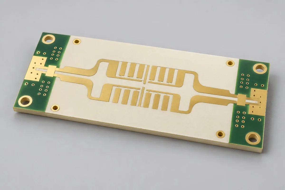
Illustrative PCB detail; not a photograph of a KFPCBA delivery

RO4350B communication PCB Historical Production Example → Metalized Half-Hole PCB →

Material and Process Reference

Consult selected PCB configuration

How should I choose Rogers high-frequency materials versus standard FR4?

FR4, RO4000, and PTFE materials cannot be compared using only the high-frequency label. First check loss, Dk models, fabrication, and flame-retardancy requirements at the target frequency and structure; compare grade prices through quotes with the same thickness and copper foil.

How should material thickness be selected for filter boards, antenna boards, and long feedlines?

Filter boards focus on coupling and resonant dimensions, antenna boards on radiation and installation, and feedline boards on transmission loss. Select a specific product in this category by application; different structures using the same material are not interchangeable boards.

High-frequency PCB pricing and selection FAQ

How much do high-frequency PCBs cost? Choosing Rogers or FR4

A project-specific quotation requires review of the available files, quantity, materials, requested tests, delivery destination, taxes, shipping, and trade terms. Add any specified processes and tests not yet included to the batch budget; these prices do not apply to other materials or layer sequences. Any formula on this page organizes cost inputs; it is not a quoted rate.View cost items, calculation conditions, and sources.

How should I compare quotations from high-frequency PCB manufacturers?

Align material grade, dielectric thickness, and copper foil before requesting quotes, and state whether the task involves filtering, radiation, or transmission. Review material price differences, hybrid lamination, and specified inspections separately; the high-frequency PCB label alone cannot support unit-price comparison.

Can high-frequency laminates with similar Dk be substituted without changing the artwork?

Retain frequency and test-method information, then check dielectric thickness, copper foil, loss, and structure. One typical parameter cannot establish equivalence; substitutions require design and manufacturing review and approval.

Should short and long feedlines use the same material?

Compare actual length, loss, and port budgets within the same frequency band. Standard materials may be considered for short paths, while long paths require loss assessment; material choice follows the task rather than the wireless label.

Can electrical testing of a bare antenna board verify radiation performance?

Electrical testing checks only agreed nets; radiation also depends on feed structures, components, and installation. Define responsible parties and data separately for bare-board fabrication and antenna-system verification.

How should an inquiry be handled if the specified high-frequency prototype material is unavailable?

Retain the original requirements and list candidate specifications, recalculation, and verification impacts; confirm first whether substitution is permitted. Temporary sample conclusions do not automatically establish a basis for the original material or production structure.

Consult high-frequency PCB quotation: describe the application, existing configuration, and expected quantity so we can discuss bare-board fabrication requirements, inspection, and delivery conditions.

Quote based on electromagnetic targets rather than part numbers

Submit frequency bands, ports, insertion-loss/return-loss or radiation targets together with copper foil and dielectric thickness. Filter boards, power-divider boards, and patch antennas have different acceptance objects: the first two concern port networks, while antennas also require installation orientation and radiation tests.

High-frequency board inquiry: frequency band and test structure

After selecting a product in this category, submit frequency bands, port reference planes, dielectric thickness, copper foil, and critical RF dimensions. Match each change to the Engineering Reference Configuration, using the same revision for fabrication drawings, inspection locations, and material approvals; define specialized verification and report scope before quotation.

Adjacent direction:High-frequency material and band products · Functionally layered mixed lamination product · Custom Rogers structure products · RF functional products

How much do high-frequency PCBs cost? Choosing Rogers or FR4

Quotes should separately account for material grade, thickness and copper foil, RF geometry, holes and surface finish, single-material or hybrid stackups, dimensions, impedance coupons, and specified inspections. List initial-order setup charges separately from per-batch and per-board charges; for equal quantities, also align revisions, delivery configurations, and tax and freight terms to identify whether price differences reflect configurations or excluded work.

Quotation terms depend on the approved files, quantity, material supply, tests and delivery requirements.

Prepare a structured RFQ or use the short inquiry form.

Quotation ItemsWhat to verify during comparison
Material Grade, Thickness, and Copper FoilGrade, thickness, and copper foil determine the procurement combination; quotes must specify the same material revision rather than merely a high-frequency substrate.
RF geometry, holes, and surface finishTransmission lines, small holes, and finish areas change manufacturing conditions; align geometric tolerances before comparing fabrication.
Single material or mixed lamination stackupSingle-material and hybrid builds differ in material usage and lamination; using less specialty material does not necessarily reduce total cost.
Dimensions, impedance coupon, and specified inspectionDefine objects and sampling for impedance coupons, dimensions, and specified reports; extra inspections are not included in board prices by default.

Need a Configuration for Your Project?

Send the materials, quantity, target date, and available files for engineering review. Review quality and acceptance, material responsibility, or use the engineering RFQ when released files are ready.

Send Requirements

Product Configurations

Compare options by material, structure, and application. Each detail page explains the process and verification conditions.

Illustrative configuration for RO4350B communications PCB configuration
Engineering Reference Configuration

RO4350B communications PCB configuration

Review RF materials, geometry, finish and measurement boundaries together. This illustrative double-sided RO4350B configuration is not a KFPCBA production example or a measured RF-performance record.

Candidate material
RO4350B; exact procurement revision and foil unverified
Illustrative construction
2 layers / 0.762 mm total board thickness; dielectric thickness must be defined separately
Candidate finish
ENIG; region and layer requirements need approval
Unverified minimum-hole callout
0.3 mm; hole type and diameter definition require drawings
View Configuration
Illustrative configuration for Rogers 5880 antenna PCB
Engineering Selection Reference

Rogers 5880 antenna PCB

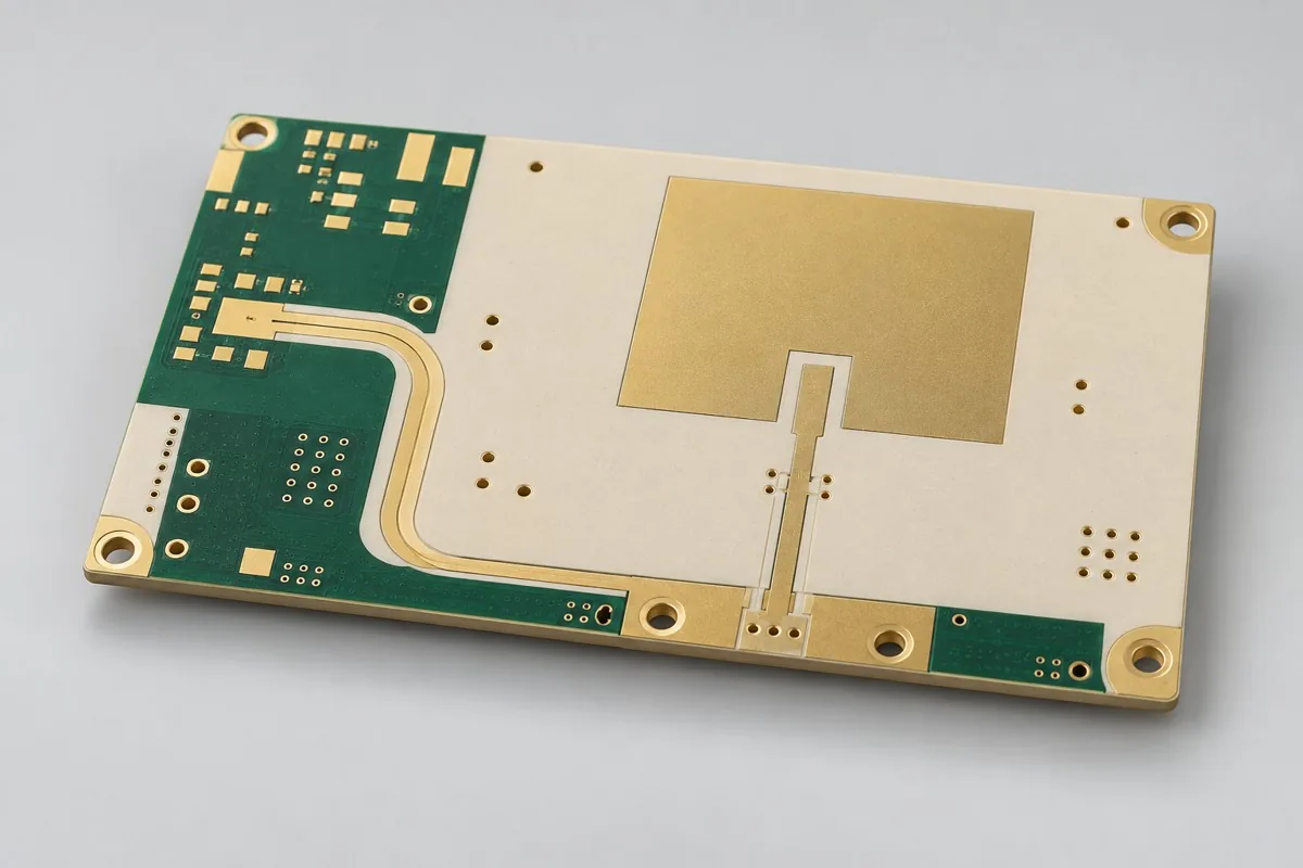
Review RT/duroid 5880 patch antenna PCB fabrication using approved radiator, feed, and ground drawings. Compare PTFE hole processing, finished copper, dimensional inspection, and optional installed antenna measurements.

Material
RT/duroid 5880
Structure
2 Layer
Specification
0.787mm Dielectric
Key Requirement
50 Ω feed
Selection Focus
Patch antenna
View Configuration
Illustrative configuration for RO3003 radar PCB fabrication
Engineering Selection Reference

RO3003 radar PCB fabrication

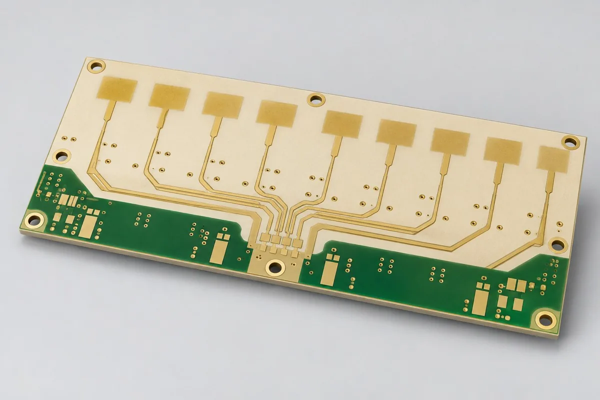
Review RO3003 antenna PCB fabrication for the illustrative 24GHz configuration. Define array coordinates, finished copper, thin-board support, dimensional tolerances, and optional de-embedded VNA or radiation measurements.

Material
RO3003
Structure
2 Layer
Specification
0.254mm Dielectric
Key Requirement
24GHz reference
Selection Focus
Array Antenna
Copper Weight
35 µm Finished Copper Target
View Configuration
Illustrative configuration for RO4835 high frequency PCB fabrication
Engineering Selection Reference

RO4835 high frequency PCB fabrication

Review RO4835 PCB fabrication for long RF feedlines. Define laminate and foil revisions, finished copper, line geometry, surface finish, and long/short-line comparison structures before agreeing loss measurements.

Material
RO4835
Structure
2 Layer
Specification
0.508mm dielectric
Key Requirement
50 Ω long feedline
Selection Focus
Immersion silver
View Configuration
Illustrative configuration for Six-layer RO4350B hybrid PCB
Engineering Selection Reference

Six-layer RO4350B hybrid PCB

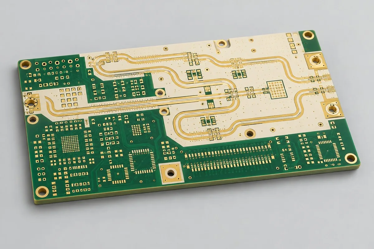
Review a six-layer RO4350B/FR4 hybrid PCB with one RF surface and digital control layers. Define RF reference planes, interface returns, lamination requirements, and separate RF and digital acceptance.

Material
RO4350B+FR4
Structure
6 Layer
Specification
1.60mm Target
Key Requirement
RF 50 Ω/differential 100 Ω
Selection Focus
Single RF Side
View Configuration
Illustrative configuration for RO4003C High-Frequency Board Prototyping
Engineering Selection Reference

RO4003C High-Frequency Board Prototyping

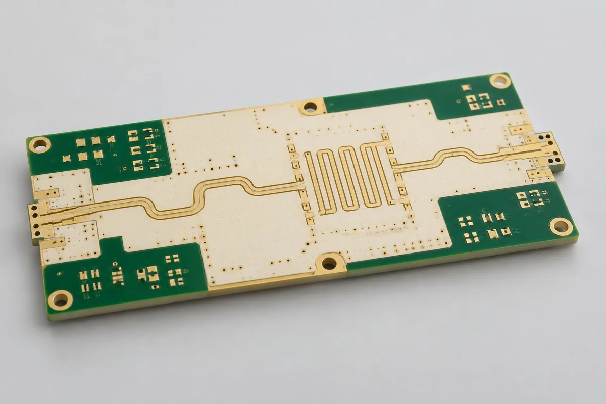
RO4003C high-frequency PCB prototyping reviews materials, structures, and deliverables against resonant/coupled artwork and material/frequency deviations, with cost breakdowns, one-time setup and same-revision reorder boundaries, configuration selection steps, and quotation conversion methods. Specifications follow approved fabrication drawings; component assembly and complete-system verification are separate.

Material
RO4003C
Structure
2 Layer
Specification
0.813mm dielectric
Key Requirement
50 Ω Port
Selection Focus
Microwave Filtering
View Configuration
Illustrative configuration for RO4350B high-frequency PCB fabrication
Engineering Selection Reference

RO4350B high-frequency PCB fabrication

RO4350B high-frequency PCB fabrication reviews materials, structures, and delivery scope against connectors, ports, and exposed-copper RF regions. It provides cost breakdowns, one-time preparation and same-revision repeat-order boundaries, configuration-selection steps, and quotation conversion methods. Specifications follow approved fabrication drawings; component assembly and complete-unit validation are agreed separately.

Material
RO4350B
Structure
2 Layer
Specification
0.508mm dielectric
Key Requirement
50 Ω Single-Ended
Selection Focus
Immersion silver
View Configuration
PCB / PCBA · PROJECT ENQUIRY

Does Your Project Need PCB Fabrication, Assembly, or Box Build?

Tell us the product use and which files are available. We can define the next engineering step even when the data package is not complete.

Call UsWhatsAppRequest a Quote