Engineering Selection Reference
RO4350B PCB fabrication: review of double-sided RO4350B RF board fabrication
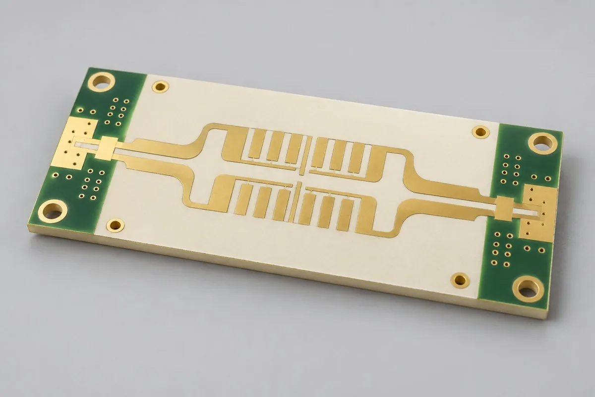
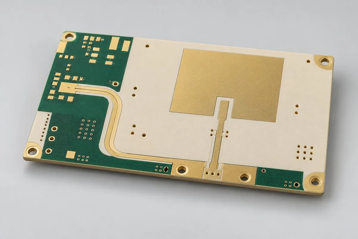
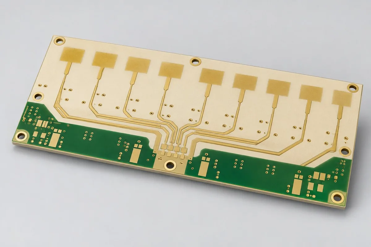
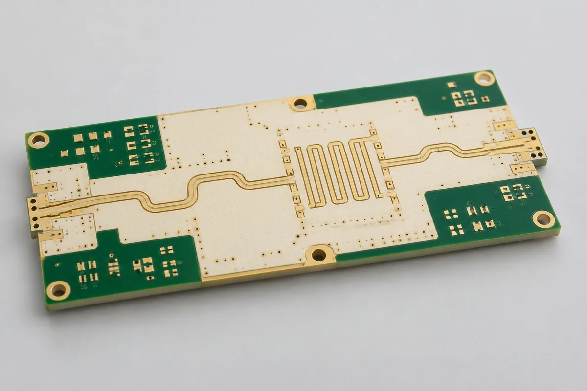
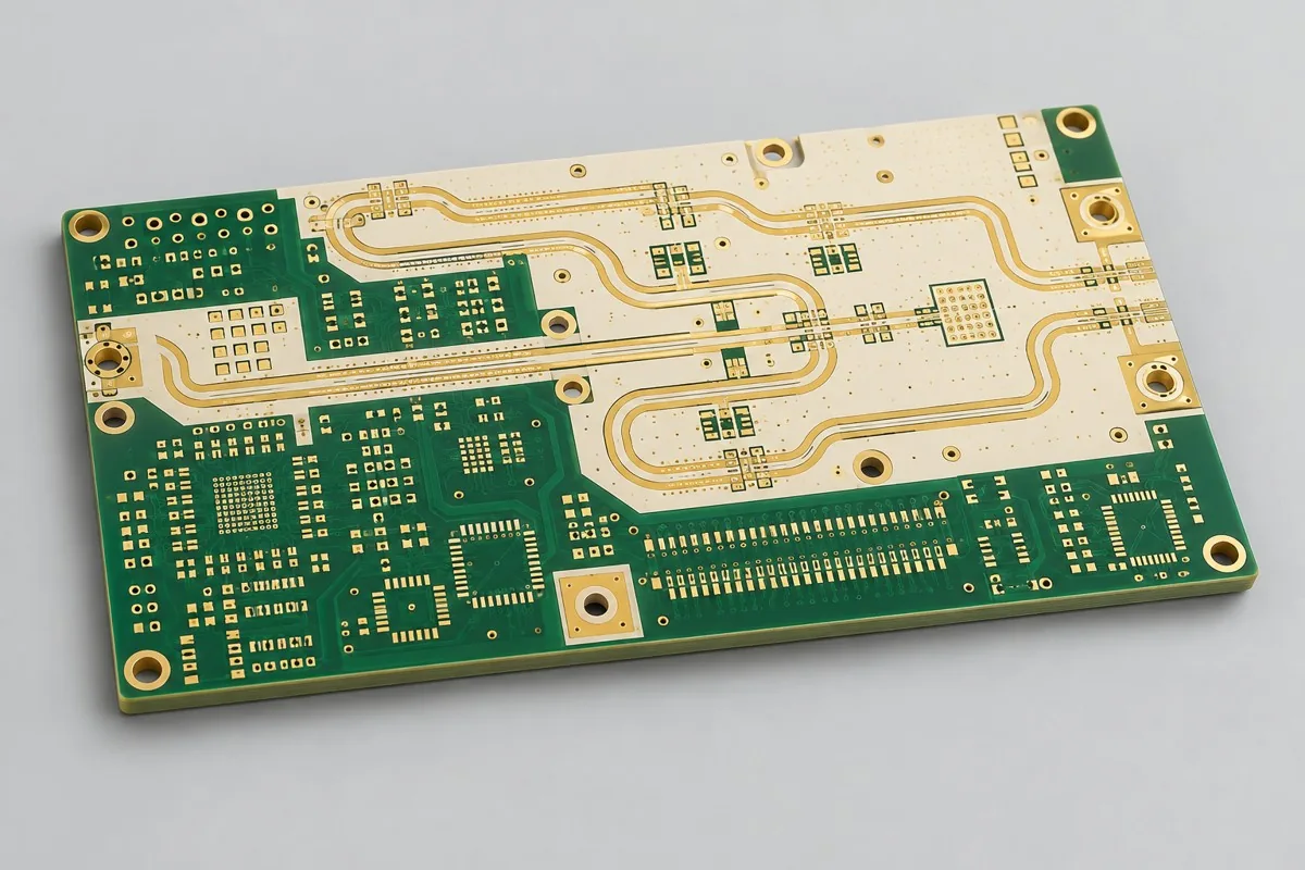
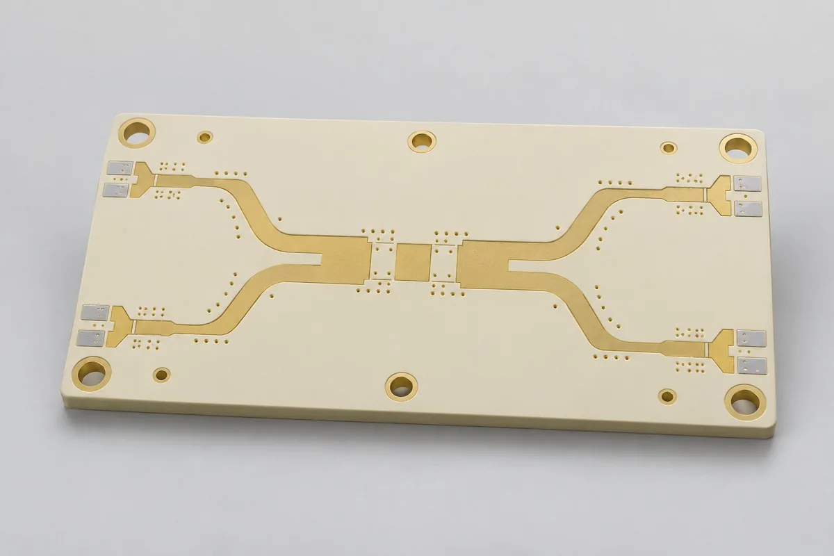
Double-sided RO4350B RF board fabrication requires review against current fabrication drawings. For bare double-sided RO4350B RF transceiver boards, freeze connector ports, continuous underside ground, and immersion-silver openings first. A 0.508mm dielectric is a reference starting point; surface-finish changes involving nickel require loss reassessment. Deliver material and geometry records, and agree separately on TDR and port VNA scope.
RO4350B PCB fabrication first requires defining bare PCB prototyping or volume-fabrication scope. Please provide Gerber data, drill files, board outline, and layer stackup, material and process requirements, quantity, and fabrication acceptance requirements. Double-sided RO4350B addresses both RF through-hole fabrication and flame-retardant material requirements
Review double-sided RO4350B RF boards first for the 0.508mm core and 50Ω microstrip; quotation inputs also need port mounting drawings and exposed-copper openings. Map critical design targets to inspection methods in the specifications and fabrication-input tables below.
Why choose this structure for bare board delivery
When RF routing occupies only one layer and the underside can retain continuous ground, a double-sided RO4350B structure puts material selection, ports, and transmission-line geometry on the same fabrication drawing. The 0.508mm dielectric is this page's selection starting point, suited to wireless front ends with room for trace width; compare RO3003 and RO4835 products separately for thin-dielectric and long-feedline projects.
How much does a RO4350B high-frequency PCB cost, and what does the quotation include?
The price of a bare double-sided RO4350B transceiver board comprises the specified 0.508mm core, patterning and hole metallization, immersion silver, profiling, electrical testing, and selected impedance or RF tests. Compare board area and panel utilization together rather than asking only for material price per square meter. List TDR coupons, connector test structures, and fixture-based VNA measurements separately to avoid mixing bare PCB fabrication quotations with complete transceiver-module pricing.
Quotation terms depend on the approved files, quantity, material supply, tests and delivery requirements.
Prepare a structured RFQ or use the short inquiry form.
Enter the following items in one itemized quotation: specify cost units and tax/shipping basis, with separate columns for first orders and same-revision repeat orders. The table is a procurement breakdown method, not a ready-made price list; reference specifications require approval against current fabrication drawings.
| Quotation items and pricing boundaries | Actual inputs requiring alignment for this model | Repurchase of same version and change boundaries |
|---|---|---|
| Materials/fabrication, quoted per batch or accepted board | Rogers RO4350B; 2 layers; base copper 35µm; finished copper target 35µm, with local copper added by hole plating accounted for separately | Recurs on repeat orders; material, layer-order, or copper-weight changes require requotation |
| Holes and forming, per approved hole table | Ø0.30mm finished through-holes; RF ground-via fence | Repeat orders follow the same-revision fabrication process; check processes before connector and port changes |
| Surface finish/packaging, noting areas and batches | Immersion silver; RF Lines Partially Exposed Without Solder Mask | Incurred by actual batch; confirm packaging, storage conditions, and surface-finish substitutions separately |
| Engineering/tooling preparation, identifying one-time or per-batch charges | Connectors and ports: include connector mounting drawings, target bands, and reference-plane locations; determine whether port compensation and test structures share the board. | Verify file revisions, ownership, and storage condition before reusing old tooling; do not assume reuse is free |
| Structural/special inspections, identifying coupons, hole groups, or samples | Agree on delivery of port dimensional checks, test-structure drawings, and calibration conditions; a 50Ω coupon cannot replace port return-loss measurements. Retain opening revisions, surface-finish batches, and packaging dates. | List initial prototype validation and per-batch sampling separately; quote per-board requirements separately rather than assuming everything is completed once |
| Delivery scope, listing reports and pass quantity | Bare PCB, material batch and RO4350B grade records, approved stackup, and dimensional/hole-wall copper sampling records; include TDR and RF test-structure data when agreed. | Retain revision links and batch records on repeat orders; list component assembly, firmware, and complete-unit testing separately |
Which costs less, RO4350B or RO4003C, and how should I choose versus FR4?
Double-sided RO4350B boards suit RF transceiver circuits over continuous ground; double-sided RO4003C filter boards emphasize coupling gaps and resonator geometry and require acceptance of non-flame-retardant material constraints. Compare FR4 for short feedlines when the loss budget permits, but dielectric changes require recalculating trace width, matching, and ports. Thickness, copper foil, quantity, and inspection scope also affect price, so there is no configuration-independent cost ranking. Compare at the same band, feedline length, and mounting conditions.
| Comparison Dimension | RO4350B high-frequency PCB fabrication | RO4003C High-Frequency Board Prototyping |
|---|---|---|
| Material and Grade | Rogers RO4350B | Rogers RO4003C |
| Layer Count and Structure | 2 Layer | 2 Layer |
| Hole Structure and Dimensions | Ø0.30mm finished through-holes; RF ground-via fence | Ø0.30mm finished ground through-holes; keep unrelated holes out of resonant regions |
| Application | Wireless transceiver modules; RF power-amplifier driver stages | Microwave bandpass filters; coupler validation boards |
Are two RO4350B layers sufficient, and when should I move to multilayer construction?
Two layers are straightforward when RF runs on one side and the underside can maintain continuous RF ground. If digital control traces fragment underside ground, RF must enter inner layers, or RF ports occupy both sides, compare six-layer single-RF hybrid, four-layer dedicated-dielectric, or eight-layer dual-RF hybrid structures separately. Draw each RF path and its ground reference before choosing layer count to control costs more effectively than choosing a high layer count first.
| Decision Sequence | This Model Input | Generated Auditable Output |
|---|---|---|
| 1 define usage and boundaries first | Include connector mounting drawings, target bands, and reference-plane locations; determine whether port compensation and test structures share the board. | Agree on delivery of port dimensional checks, test-structure drawings, and calibration conditions; a 50Ω coupon cannot replace port return-loss measurements. |
| 2 fixed conditions affecting structure | Identify immersion-silver regions, solder-mask keepouts, and the wait before assembly; separate protective packaging and surface-finish options in the quotation. | Retain opening revisions, surface-finish batches, and packaging dates. |
| 3 Align Networks with Manufacturing Targets | 50Ω single-ended; microstrip/coplanar model + impedance-coupon TDR | Provide target nets, layer pairs, and validation scope; review together with Ø0.30mm finished through-holes and the RF ground-via fence |
| 4 then verify quotation and release | Rogers RO4350B; 0.58mm target (excluding solder mask); immersion silver; selected RF traces without solder mask | Request quotations using material/pattern/inspection lists at the same revision; list unapproved substitutions as separate alternatives rather than including them in the baseline quotation |
Ship Bare Board Manufacturing Specs
| Specification Items | Clarify Configuration/Target |
|---|---|
| Material and Grade | Rogers RO4350B |
| Layer Count and Structure | 2 Layer |
| Total Board Thickness | 0.58mm target (excluding solder mask) |
| Dielectric thickness and interlayer relationship | 0.508mm core board |
| Base Copper and Finished Copper | Base copper 35µm; finished copper target 35µm, with local copper added by hole plating accounted for separately |
| Hole Structure and Dimensions | Ø0.30mm finished through-holes; RF ground-via fence |
| Trace Width and Spacing | 0.15/0.15mm reference minimum design; RF trace width determined by field solving |
| Impedance Target and Measurement Methods | 50Ω single-ended; microstrip/coplanar model + impedance-coupon TDR |
| Surface Finish | Immersion silver; RF Lines Partially Exposed Without Solder Mask |
| Original Material Specifications | RO4350B: process Dk 3.48±0.05, design Dk 3.66; Df 0.0037 (10GHz, manufacturer typical values) |
| Application | Wireless transceiver modules; RF power-amplifier driver stages |
| Deliverables | Bare PCB, material batch and RO4350B grade records, approved stackup, and dimensional/hole-wall copper sampling records; include TDR and RF test-structure data when agreed. |
Incoming/outgoing bare board layer sequence and hole structure
The following shows functional layer order/material structure for this reference configuration, not a production stackup drawing; do not infer thickness from graphic proportions. Match copper-layer numbering to via layer pairs item by item in approved fabrication files.
| Top to Bottom | Layer Responsibilities/Structure |
|---|---|
| L1 | RF signal and matching pads |
| L2 | Continuous RF Ground |
Hole structure: Ø0.30mm finished through-holes; RF ground-via fence
RO4350B dielectric and loss models
RO4350B process Dk supports material comparisons; transmission-line or resonator models use design Dk for the applicable frequency and method. Freeze procurement thickness, copper foil, and surface-finish revisions together. Return first-article measured geometry to design for review; material Df is only an input to the loss budget.
Trade-offs between immersion-silver protection and nickel-layer loss budgets
RO4350B is primarily selected for controlled dielectric properties and a well-established thermoset fabrication route. It cannot compensate for abrupt connector-pad transitions, narrow ground-return paths, or insufficient power-amplifier device cooling. Immersion silver is the reference finish and is susceptible to packaging and contact contamination; if changed to ENIG, include nickel on critical traces in the loss budget again.
RF etched trace width and ground-via fences: fabrication inspection
Control post-etch RF trace width, copper weight, and ground-via spacing rather than reporting minimum trace width alone. Retain a complete underlying ground at connector transitions, keep solder-mask opening edges away from impedance-sensitive sections, and fabricate impedance coupons with the same core batch, same-side copper, and same surface finish.
Separate acceptance of TDR coupons and connector-port VNA measurements: acceptance items
Check bare PCBs for continuity/shorts and dimensions; compare impedance coupons against design targets using TDR. Measure RF performance with VNA on test structures fitted with specified connectors. State numerical test bands, reference planes, and permitted insertion loss/return loss in the order; a passing 50Ω coupon cannot establish complete-unit RF compliance.
Ship Bare Board Delivery Scope
Applications: wireless transceiver modules; RF power-amplifier driver stages.
Bare PCB, material batch and RO4350B grade records, approved stackup, and dimensional/hole-wall copper sampling records; include TDR and RF test-structure data when agreed.
Port mounting drawings and exposed-copper openings: RFQ inputs
Submit port mounting drawings and exposed-copper openings to turn tabled design targets into inspectable fabrication drawings. The following inputs define pattern, material, or structural inspection scope; freeze the quotation revision with approved drawings.
| Inputs required to be completed for this product | Engineering Decisions Affected | Records/delivery as agreed in the order |
|---|---|---|
| Connectors and Ports | Include connector mounting drawings, target bands, and reference-plane locations; determine whether port compensation and test structures share the board. | Agree on delivery of port dimensional checks, test-structure drawings, and calibration conditions; a 50Ω coupon cannot replace port return-loss measurements. |
| Exposed Copper RF Area | Identify immersion-silver regions, solder-mask keepouts, and the wait before assembly; separate protective packaging and surface-finish options in the quotation. | Retain opening revisions, surface-finish batches, and packaging dates. |
RO4350B high-frequency PCB fabrication: pricing, selection, and procurement FAQ
How much does a RO4350B high-frequency PCB cost, and what does the quotation include?
A project-specific quotation requires review of the available files, quantity, materials, requested tests, delivery destination, taxes, shipping, and trade terms. Add any specified processes and tests not yet included to the batch budget; a quotation for this configuration does not apply to other materials or layer sequences. Any formula on this page organizes cost inputs; it is not a quoted rate.View cost items, calculation conditions, and sources.
Which costs less, RO4350B or RO4003C, and how should I choose versus FR4?
RO4003C and RO4350B cannot be ranked uniformly by price using grade names alone; align thickness, copper foil, quantity, and testing. RO4003C filter structures require acceptance of non-flame-retardant material conditions; RO4350B suits transceiver paths that also require flame-retardant materials. Compare FR4 for short feedlines only when the loss budget permits. View Specific Comparison Basis
Are two RO4350B layers sufficient, and when should I move to multilayer construction?
If RF occupies one side and the other retains continuous reference ground, evaluate two layers first. When digital traces fragment underside ground, RF enters inner layers, or both sides have RF ports, compare single-RF hybrid, all-dedicated multilayer, or dual-RF hybrid structures separately instead of adding layers without a purpose. View Specific Comparison Basis
Can RO4350B prototypes be changed directly to ENIG?
ENIG can be compared as an option, but nickel on RF traces and the solder-mask environment change the loss model. Check pad solderability and long-feedline losses separately; do not retain the original RF pattern and merely change the surface-finish name.
Where do RO4350B volume-production savings versus prototypes come from?
With the same materials and drawings, file processing, test preparation, and panelization can be spread across more accepted boards in volume production. If per-board VNA testing is added or board shape changes at the same time, unit prices may not fall proportionally with quantity.
Which reports should I review when selecting a RO4350B fabricator?
Review grade and batch records, approved dielectric thickness, RF etched dimensions, and coupon layer pairs; RF acceptance also requires port reference planes and calibration methods. A 50Ω coupon report alone cannot assess connector transitions and insertion loss across the entire path.
Which costs can be saved by using TDR without VNA on a RO4350B transceiver board?
The order can specify only bare PCB electrical testing, dimensions, and TDR coupons, excluding connector installation, port-fixture preparation, and VNA measurements. This reduces RF validation scope; it does not establish compliant ports. If release requires return loss or insertion loss, retain the corresponding test structures and reference planes.
How can per-board and per-panel quotations for RO4350B high-frequency PCB fabrication be converted?
Panel drawings should show RF ground-via fences, ports, and impedance coupons together; check depaneling edges and SMA mounting locations. List packaging protection for immersion-silver exposed-copper regions separately. Specify deliverable finished-board quantity per panel, actual panel purchasing quantity, and individual-board/panel delivery state. Calculate fabrication cost per board by dividing actual panel fabrication cost by the corresponding accepted finished-board quantity; list preparation, special inspection, and packaging separately. Theoretical utilization cannot promise yield.
How should first-order one-time costs and repeat-order costs be separated for RO4350B high-frequency PCB fabrication?
For the first order, confirm documentation for connectors, ports, and exposed-copper RF regions, identifying whether related engineering, tooling, or test preparation is charged once. Agree on delivery of port dimensional checks, test-structure drawings, and calibration conditions; a 50Ω coupon cannot replace port return-loss measurements. Before reusing tooling, verify files and ownership. This batch still incurs materials, fabrication, and approved inspections; separately list preparation that must be repeated after changes rather than relying on the old order total.
Can I get a RO4350B high-frequency PCB fabrication budget before connector and port information is complete?
Start with the application, board outline, quantity, and available drawings to obtain a budget identifying missing inputs. Formal review for this product requires connector mounting drawings, target bands, and reference-plane locations, and a decision on whether port compensation and test structures share the board. Corresponding deliverables are agreed port dimensional checks, test-structure drawings, and calibration conditions; a 50Ω coupon cannot replace port return-loss measurements. Confirm fabrication/inspection quotations after these conditions are frozen. Initial inquiries need not include every file, but estimates do not imply coverage of undefined structures.
What must be reconfirmed when changing materials, hole tables, or mounting conditions on repeat orders for RO4350B high-frequency PCB fabrication?
Identify immersion-silver regions, solder-mask keepouts, and the wait before assembly; separate protective packaging and surface-finish options in the quotation. Retain opening revisions, surface-finish batches, and packaging dates. Match each changed location against prior material/hole-table/mechanical files to determine whether drawings, processes, or measurements need updating. Retaining only the product name and layer count cannot establish identical repeat-order conditions.
When two RO4350B high-frequency PCB fabrication quotations specify the same material, which configurations still need checking?
Compare the 0.508mm core, RF finished copper, and immersion-silver openings first. TDR coupons and port VNA measurements are different scopes; quotations including connectors/fixtures cannot be compared directly with bare PCB prices.
Which reports should link to board IDs before RO4350B high-frequency PCB fabrication moves from prototypes to volume production?
Agree on delivery of port dimensional checks, test-structure drawings, and calibration conditions; a 50Ω coupon cannot replace port return-loss measurements. Retain opening revisions, surface-finish batches, and packaging dates. Link material batches, approved fabrication files, and these inspection results to current prototype IDs; use the revision with issues closed for volume production. Reports for old coupons or patterns support comparison but cannot replace current fabrication inputs. Define separate scope for complete-unit items not yet covered.
If small-batch RO4350B high-frequency PCB unit prices fall, how can I determine whether total procurement costs really decrease?
For the same batch of transceiver boards, compare separate quotations for bare PCBs/TDR only and for added connector VNA testing; the former removes RF port validation and cannot be called a price reduction at equal scope. Total preparation, fabrication, agreed inspection, packaging, and shipping, then divide by the accepted delivery quantity to compare total and per-board costs at equal scope. Use current RFQ amounts and rates rather than assuming a fixed reduction.
Comparison of bare boards with adjacent board types
Current configuration distinction: double-sided RO4350B addresses both RF through-hole fabrication and flame-retardant material requirements
- RO4003C double-sided microwave filter board — Thicker double-sided RO4003C resonator structure, focusing on coupling gaps and center frequency
- RT/duroid 5880 low-Dk patch antenna board — Low-Dk PTFE radiating structure, with dimensions and hole treatment different from double-sided filter boards
- RO3003 thin-dielectric 24GHz radar antenna board — Thin ceramic-filled PTFE dielectric addressing fabrication deviations in 24GHz feedlines/arrays
- RO4835 low-loss long-feedline filter board — RO4835 material and copper-foil options emphasize long-trace loss/material-aging validation
- Six-layer RO4350B RF/digital hybrid interface board — A functionally integrated option in the high-frequency category, with a single RF layer + digital-ground isolation, distinct from material-focused boards
High-frequency PCB complete product catalog · All PCB Products
Design and Assembly Responsibilities for Incoming Bare Boards
Related Functional Directions:RF Transceiver Interface Board · RF transceiver gain and bias board design. These pages compare design or assembly responsibilities in the same application area. Materials, layer counts, components, and interface configurations differ; they do not share one physical model and are not extended delivery records for this engineering reference configuration.
Bare PCB validation on this page covers agreed materials, patterns, continuity/insulation, stackup, and test coupons. Design work separately covers circuits, models, and drawings; PCB assembly separately covers BOM components, soldering, firmware, and post-assembly functional tests. Before moving to related services, remap scope using final drawings/BOM; bare PCB reports cannot replace complete-unit acceptance.
Bare board materials and design basis
- Engineering reference | RO4350B material: high-frequency parameters and stackup confirmation: Published manufacturer material data
- Engineering reference | General high-speed interface layout: return paths, length, and layer transitions: Design methodology
When citing the above materials, record material revisions and design conditions for the 0.508mm core and 50Ω microstrip; first-article review should distinguish TDR coupon acceptance from connector-port VNA acceptance. If materials, copper weight, or via structure change, update fabrication drawings and inspection items before release.
Request Quote for This PCB Configuration: reference product ID 216, include critical circuits/interfaces and quantity, and identify specifications to retain or adjust.