Company Address
201, Factory 6, Longhui Industrial Park, Fuqiao 3rd District, Xinhe Community, Fuhai Street, Baoan District, Shenzhen, Guangdong, China

NEWS & ENGINEERING

PCB Fabrication Knowledge

Explore PCB fabrication guides on materials, stackups, vias and prototype planning. Connect design files with manufacturing and acceptance requirements.

Engineering Resources

PCB · PCB ASSEMBLY · DESIGN · PROCUREMENT AND ACCEPTANCE

PCB Fabrication Knowledge

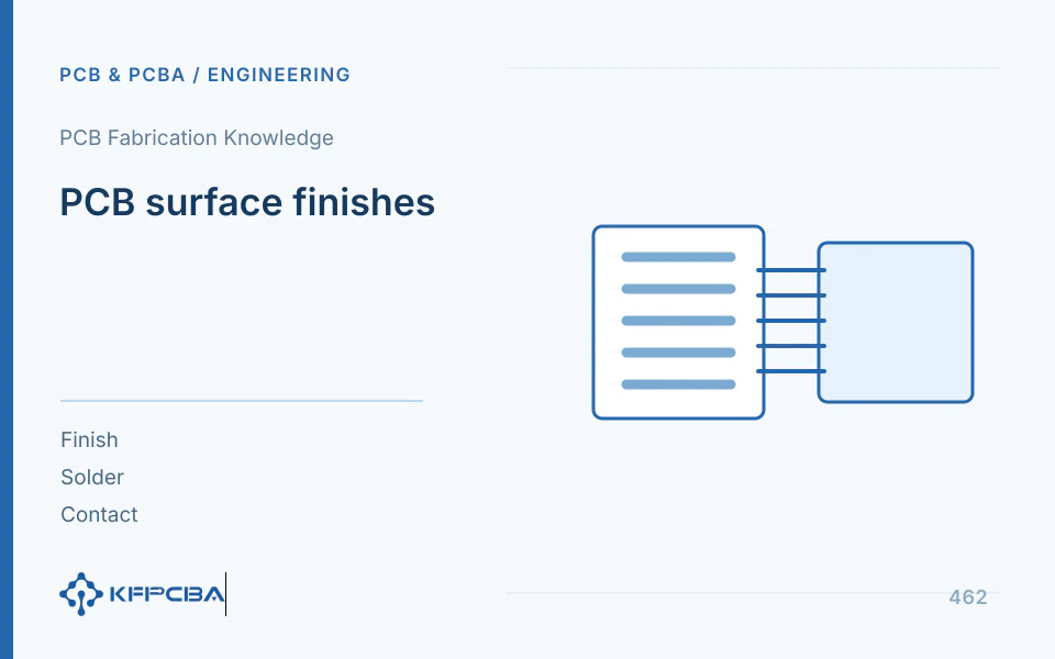
PCB surface finishes: soldering, contact, and storage requirements

Select PCB surface finishes by region according to soldering, contact, and storage requirements. This article compares priorities for HASL, OSP, ENIG, immersion tin, immersion silver, and contact gold. A split-bag opening example explains inventory management, with records for coating-thickness definitions, region boundaries, and soldering-failure troubleshooting.

Read Article
PCB Fabrication Knowledge

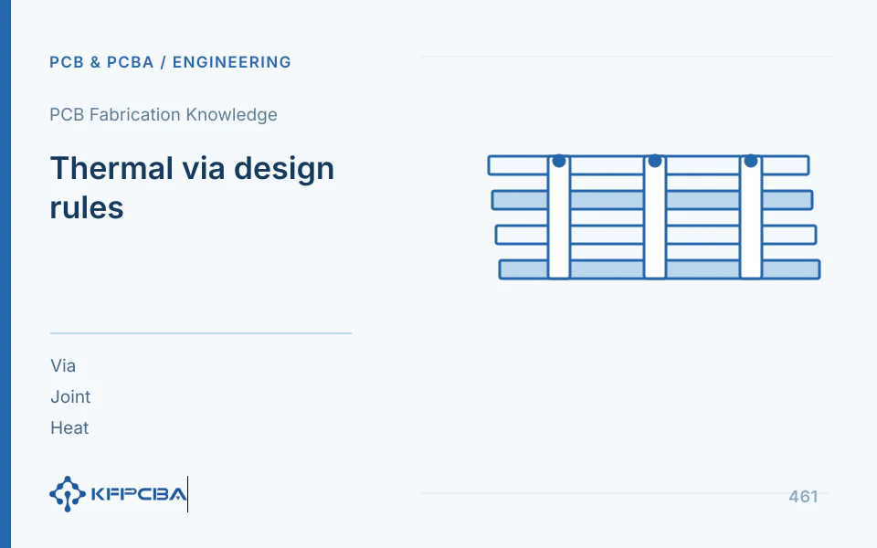
Thermal via design rules: hole-wall copper, fill, and interface contact

Thermal vias require joint review of hole-wall copper, fill, soldering, and external contact. This article uses hole-wall copper cross-sections and parallel thermal-path calculations to explain the limits of adding vias, with via-array configurations, stencil coordination, and measurement tables for diagnosing solder loss, voids, interface air gaps, and unchanged temperature rise.

Read Article
PCB Fabrication Knowledge

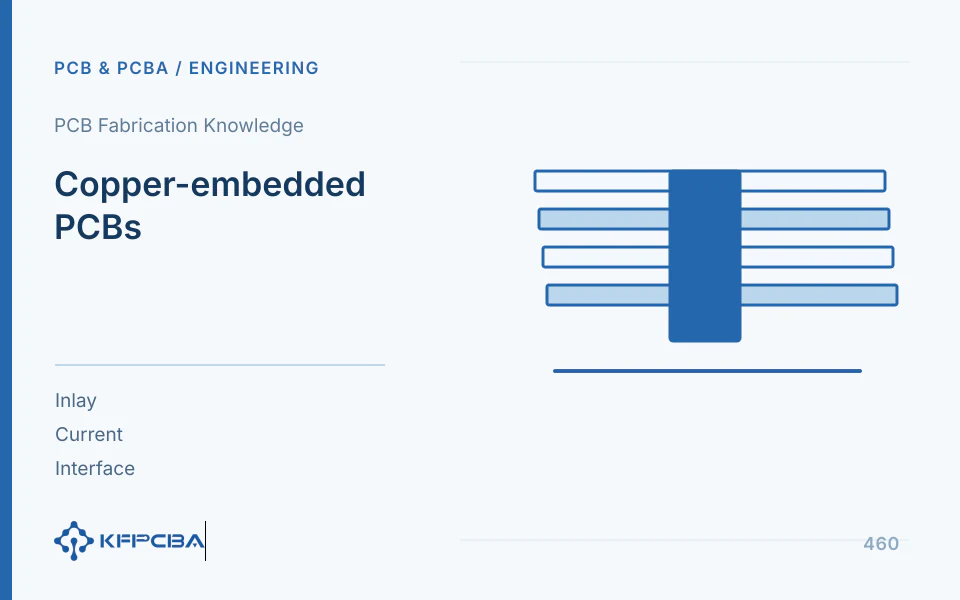
Copper-embedded PCBs: high-current cross-sections and local heat transfer

Embedded copper connects high-current or heat-transfer regions through local cross-sections; its capacity cannot be determined from copper weight alone. This article uses cross-section, resistance, and dissipation calculations to illustrate connection bottlenecks, and provides three-dimensional structural inputs, insulation and lamination checks, four-wire voltage-drop measurements, and local hot-spot troubleshooting.

Read Article
PCB Fabrication Knowledge

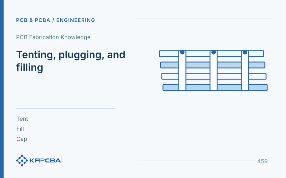
Tenting, plugging, and filling: specifying via-in-pad requirements

Tenting, plugging, filling, and copper capping correspond to different cross-sections; via-in-pad requirements cannot be defined by 'plugging' alone. This article compares hole treatments for preventing solder wicking, planarity, protection, and assembly, uses a hole-volume calculation to illustrate dimensional effects, and provides hole-group tables, inspection methods, and solder-loss troubleshooting.

Read Article

PCB Fabrication Knowledge

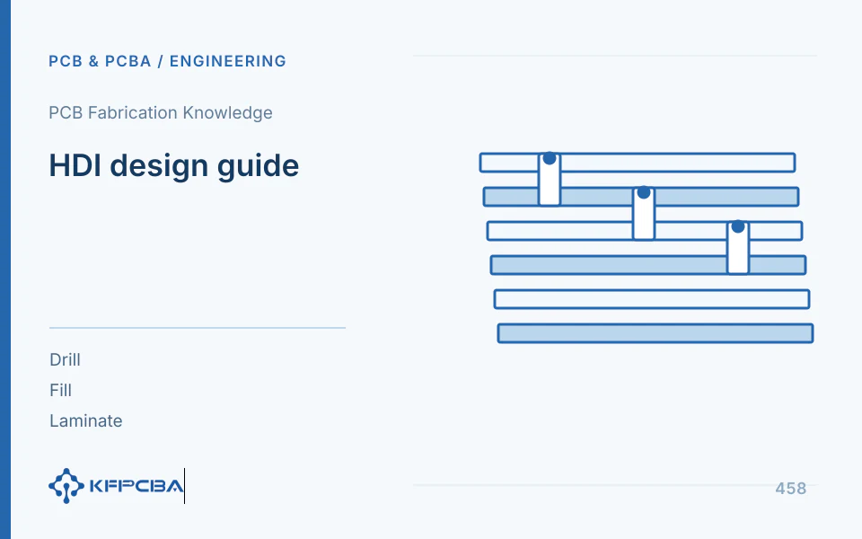
HDI design guide: microvias, via filling, and layer-sequence checks

An HDI fabrication review must check each microvia group's start and end layers, depth, fill, stacked interfaces, and lamination sequence. This article uses an eight-layer via configuration and an aspect-ratio calculation to explain documentation methods, with checklists for fabrication inputs, representative cross-sections, and fault localization. It distinguishes copper-filled microvias, resin-filled vias, and tented vias.

Read Article
PCB Fabrication Knowledge

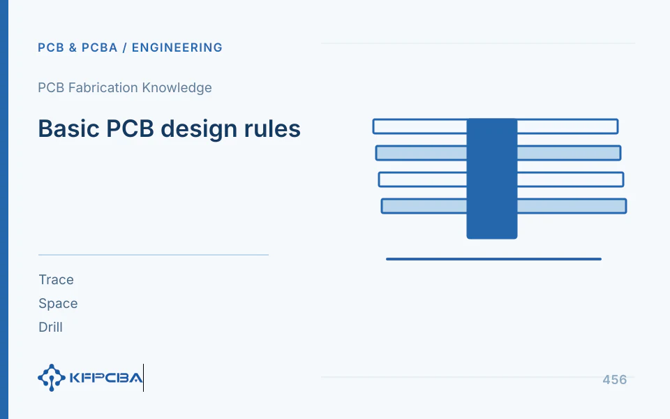
Basic PCB design rules: copper weight, spacing, and hole size

PCB rules must match copper weight, hole types, materials, and tolerances rather than uniformly smaller clearances. Annular-ring/routing-channel examples explain dependencies, with grouped CAD rules, exception closure, and fabrication review, distinguishing manufacturing rules from electrical spacing.

Read Article
PCB Fabrication Knowledge

HDI microvia structures: breakout density and sequential lamination

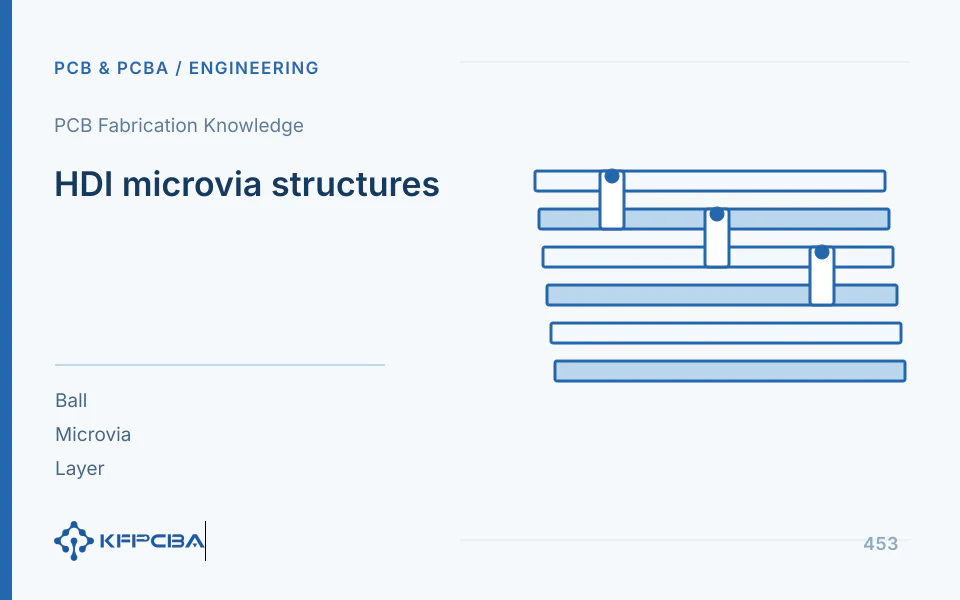
Determine HDI order from actual BGA breakout, references, and via layer pairs. This article compares through-hole dogbones, microvia dogbones, and microvias in pads, using routing-width examples to identify bottlenecks. Sequential-lamination, stacking tradeoffs, and verification inputs prevent structure upgrades based only on package pitch.

Read Article
PCB Fabrication Knowledge

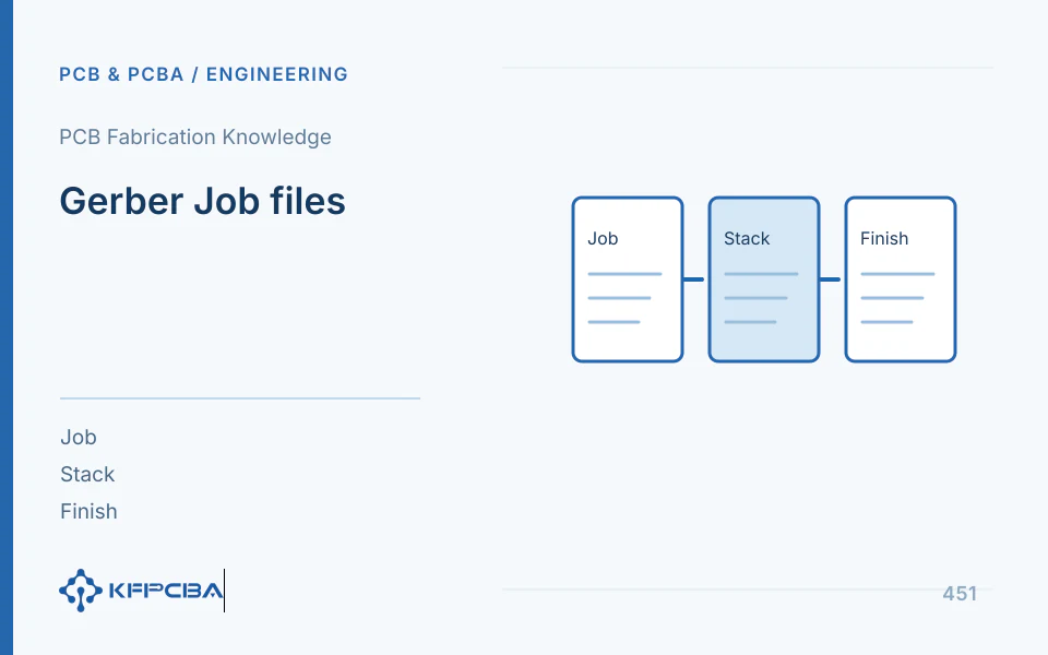
Gerber Job files: manufacturing attributes and package consistency

Gerber Job provides machine-readable manufacturing attributes but cannot automatically resolve thickness, finish, or layer-order conflicts. A Job/drawing thickness mismatch illustrates attribute comparisons, referenced-file completeness, complete-package reissue, and checksum records, defining partial-implementation boundaries.

Read Article

PCB fabrication resources: understanding fabrication through structures and materials

HDI structure and low-volume material preparation involve two separate decisions: define via layer pairs and build-up layers, then assess how material availability and substitutions affect validation.

PCB / PCBA · PROJECT ENQUIRY

Does Your Project Need PCB Fabrication, Assembly, or Box Build?

Tell us the product use and which files are available. We can define the next engineering step even when the data package is not complete.

Call UsWhatsAppRequest a Quote