Engineering reference design · prototype validation pending
WiFi/Bluetooth core board design: UART/SPI to Wi-Fi/Bluetooth access
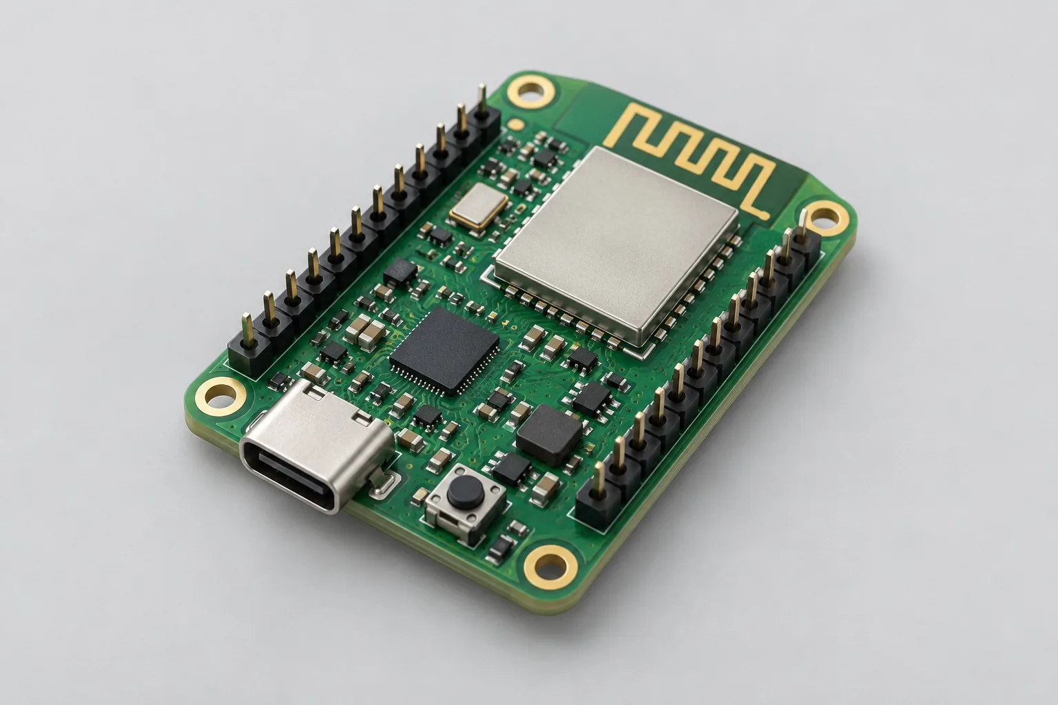
The Wi-Fi/Bluetooth communication core board connects UART/SPI devices to Wi-Fi and Bluetooth; the controller buffers data, configures networks, forwards data, and recovers from disconnections. Evaluate four-layer through-hole construction within compact outlines first, then compare HDI if package breakout is constrained.
Custom development reference design. The parameters below are requirement configurations and design targets; validate product performance through agreed prototype tests.
| Functional Partition | Design and verification scope |
|---|---|
| Wireless Antenna Area | Freeze antenna type, clearance, and enclosure-metal positions; inspect module and external antennas by actual revision. |
| Wi-Fi / Bluetooth module | Choose ESP32-S3 modules or ICs, distinguishing Wi-Fi/Bluetooth protocols and connection roles and following their layout requirements. |
| MCU Application and Interface | Define UART/SPI frames, flow control, buffer depth, and wireless forwarding; list I²C expansion and USB debugging separately. |
| Extension/debug interface | Retain programming, logging, and recovery access; check USB/peripheral levels, pinouts, and powered-off states. |
| Peak Power Supply and Decoupling | Design 5V-to-3.3V power for wireless transmit peaks; measure transient voltage drops and reset causes at the module. |
| Enclosure/antenna clearance | Check antenna direction and coverage differences inside enclosures; link throughput, reconnection, and concurrency conditions to firmware/antenna revisions. |
How much does WiFi/Bluetooth core board design cost, and how is it quoted?
Distinguish module and bare-IC approaches first. Module integration focuses on power, interfaces, and wireless bridging; bare ICs add crystal and RF-layout debugging. HDI for constrained packages also changes design/prototype costs. Network configuration, disconnection recovery, and apps are different costs; compare required functional endpoints.
Quotation terms depend on the approved files, quantity, material supply, tests and delivery requirements.
Prepare a structured RFQ or use the short inquiry form.
| Quotation Items | What services are included | What to Check When Comparing Quotes |
|---|---|---|
| Circuit and PCB Design | Wireless module/bare-IC selection, antenna clearance, and compact breakout | Reusable portions of existing designs and circuit/mechanical changes |
| Software and Validation | Bridge firmware and disconnection recovery | UART/SPI bridging, wireless network configuration, and mobile apps are separate development items |
| Prototype Preparation | Bare PCB, BOM procurement, assembly, and agreed prototype quantity | Whether material/component revisions, prototype quantities, and test targets match |
| Subsequent Revision | Record new requirements separately from post-test corrections | How agreed changes, source files, and validation results are delivered |
Are modules or bare ICs more cost-effective for WiFi/Bluetooth core boards?
Modules reduce RF integration and suit early application validation; bare ICs require crystals, RF matching, and fuller layout debugging. Compare development effort, board space, and expected-volume materials rather than IC procurement alone.
Do smaller WiFi/Bluetooth boards always need HDI?
Check package ball pitch, breakout, and antenna clearance first. If module placement or mechanical adjustments enable routing, size alone does not justify microvias. Compare HDI and conventional multilayer construction when connections and reference planes cannot otherwise fit.
Does a WiFi/Bluetooth core board quotation include a mobile app?
UART/SPI bridging, wireless network configuration, and mobile apps are separate development items. List core-board firmware, application interfaces, apps, and cloud requirements separately; wireless access does not automatically include complete phone software.
Reference configuration: UART/SPI to Wi-Fi/Bluetooth access
| Configuration Field | Reference Configurations/Selections | Basis and Status |
|---|---|---|
| Finished Product Function | UART/SPI devices connecting to Wi-Fi and Bluetooth | Design Objective |
| Wireless Configuration | Choose ESP32-S3 module or IC approach | Design Objective |
| Power Supply Objective | 5V input to 3.3V wireless domain | Design Objective |
| External Interface | UART, SPI, I²C, and USB debugging | Design Objective |
| Storage Planning | Select Flash/PSRAM for the actual component combination | Design Objective |
| Board-outline target | 35×30mm target, including antenna keepout | Design Objective |
| Stackup Candidate | Prioritize 4-layer through-holes; evaluate 6-layer 1+4+1 HDI for constrained breakout | Design Objective |
| Antenna Solution | Module onboard antenna or external IPEX antenna | Design Objective |
| Component Package | Module pads/QFN; verify footprint libraries item by item | Design Objective |
| Firmware Delivery | Communication bridging, network configuration, status logs, upgrade interfaces | Design Objective |
| Assembly Focus | Bottom pads, stencil apertures, and module soldering flatness | Design Objective |
| Validation outputs | Throughput/packet-loss, power-transient, and complete-unit antenna test plans | Design Objective |
Module, bare-IC and HDI options
A module reduces RF matching work; a bare-IC approach adds crystal, power, and antenna development.
HDI only addresses package-breakout or board-outline bottlenecks; a communication label does not require blind vias.
Separate application firmware from wireless-stack interfaces; accept device buffering and retransmission after disconnection separately.
Design budget and trade-off examples
Check design targets with engineering calculations
If module current rises from 80mA to 400mA and equivalent supply/routing resistance is 0.2Ω, the resistive voltage-drop increase alone is (0.4-0.08)×0.2=64mV.
Conditions and Scope of Application:Transients also depend on supply dynamics, capacitor ESR, and interconnect inductance; record probe positions and load states. 64mV is not an allowed-drop limit.
Replace examples with selected components and record margins; calculations support design choices, while prototype records support acceptance.
Power and layout for UART/SPI to Wi-Fi/Bluetooth access
- Draw antenna/enclosure keepouts first, then place modules and connectors; decouple wireless power near its entry.
- Use staggered connections for candidate blind-via structures and review filling requirements; do not stack microvias without fabricator approval.
- Maintain reference planes for USB and high-speed memory traces; keep crystal loops and antenna feedlines away from switching nodes.
Communication core board development input
- Wireless protocols, data volume, and connected-device count
- Board outline, enclosure-metal positions, antenna positions
- Selected module/IC models and Flash/PSRAM capacity requirements
If circuit files exist, provide editable schematics, PCB, BOM, and current issues, and agree on review or revision scope. If only functions are defined, freeze this page's inputs before selection and circuit development. Agree separately on control-software and external-application responsibilities, interfaces, and acceptance.
Communication core board phase delivery
| Stage | Engineering Work for This Proposal | Reviewable Deliverables |
|---|---|---|
| Requirements and Design Freeze | Freeze UART/SPI data volume, wireless roles, connection count, and board/antenna positions | Functional/interface requirements, mechanical revision, acceptance conditions, and open items |
| Schematic and Component Selection | Complete wireless MCU, Flash/PSRAM, bridge interfaces, programming access, and power circuits | Editable schematics, controlled BOM, footprint checks, and design calculations for these circuits |
| Layout and Routing | Compare through-hole/microvia breakout; implement antenna copper keepouts, decoupling, USB, and memory net constraints | PCB source files, actual stackup/hole/net constraints, DRC, and assembly-dimension checks |
| Simulation/Calculation | Budget buffering, sustained throughput, and peak power; assess HDI need from packages | Design calculations/models, input conditions, margins, and items awaiting measurement |
| Prototype and Software | Build core-board prototypes and integrate UART/SPI bridging, network configuration, Bluetooth connections, and upgrade recovery | Fabrication package, communication core-board prototypes, bridge/configuration firmware, serial-frame protocols, and programming/upgrade recovery instructions |
| Testing and Version Closure | Validate frame integrity, reconnection, concurrent transmission/reception, voltage drop, and in-enclosure antenna performance | Procedures, wiring, raw results, and decisions for the prototype revision; include issue/change and limitation lists |
Wireless bridging and recovery verification
- Voltage-drop and reset checks at transmit-current peaks
- Network configuration, reconnection after network loss, and interrupted-upgrade recovery
- In-enclosure wireless transmission/reception and directional coverage assessment
- Package soldering, edge antennas, and microvia prototype manufacturability review
Validate frame integrity, reconnection, concurrent transmission/reception, voltage drop, and in-enclosure antenna performance. Record equipment, conditions, revisions, and criteria in reports, identifying passed and uncovered items.
Wireless bridging and recovery verification worksheet
The table below turns UART/SPI-to-Wi-Fi/Bluetooth access into executable checks. Freeze samples, equipment, environment, and permitted deviations before execution; link results to this revision's raw records.
| Verification Object | Pre-Production Freeze | How to Test Prototypes in Practice | Delivery and Acceptance Records |
|---|---|---|---|
| Module/Chip Routing Paths | Target throughput, module model, antenna approach, mechanical keepouts | Compare space, debugging, and production tests for selected module and IC approaches | Deliver approach comparisons and breakout review without HDI; actual module documentation defines keepouts |
| Wireless and Power Supply | Network type, reporting load, supply range, and permitted reset strategy | Run continuous transmission/reception and reconnection inside enclosures, capturing peak power responses | Retain throughput/reconnection times, module voltage drops, and reset causes; link each result set to firmware/antenna revisions |
| Upgrade Recovery | Upgrade access, image revisions, and interrupted-upgrade rollback rules | Interrupt power during downloading, writing, and image switching separately | Record boot partitions, recovery, and configuration retention; accept each agreed recovery path separately |
Manufacturing and assembly coordination for this design
- Compare through-hole and HDI cost/yield risks first; select HDI only when space constraints justify it.
- Clearly mark module-antenna copper keepouts, via filling, and solder-inspection locations in fabrication files.
Link design revisions to schematics, BOM, PCB, fabrication, and software documentation. Recheck critical electrical and test conditions when fabricators adjust stackup, materials, or holes or assemblers propose substitutes.
Common questions on purchasing and customization
How much does WiFi/Bluetooth core board design cost, and how is it quoted?
A project-specific quotation requires review of the available files, quantity, materials, requested tests, delivery destination, taxes, shipping, and trade terms. Complete development separately prices circuits, firmware, prototypes, and verification. Any formula on this page organizes cost inputs; it is not a quoted rate.View cost items, calculation conditions, and sources.
How should WiFi/Bluetooth boards test disconnection recovery?
Under specified router/phone conditions, record connection, disconnection, reconnection, and buffered data, distinguishing network faults from device power resets.
Does changing a WiFi board enclosure require revalidation?
Recheck antenna clearance and installation positions and measure communication inside the new enclosure; bare-board debug records do not directly establish in-enclosure performance.
How should WiFi/Bluetooth board development budgets compare modules and ICs?
For the 35×30mm target, UART/SPI access, and actual enclosure, define two work packages. Module versions check antenna clearance and bridging; IC versions add crystals, matching, and RF debugging. Align prototypes, network configuration, and in-enclosure communication tests before comparing development effort and subsequent materials, rather than module/IC prices alone.
Can layout alone be commissioned when complete ESP32 reference circuits exist?
Layout can be discussed after freezing the selected ESP32-S3 module/IC, Flash/PSRAM combination, 5V-to-3.3V capability, and antenna structure. Reference circuits do not define customer-enclosure clearances or bridge protocols; itemize unfinished circuit review and firmware tasks separately.
What bridge-firmware work remains if customers provide an app?
Customers must provide network-configuration entry, device discovery, data frames, and disconnection strategies. Boards still need UART/SPI buffering, wireless-state handling, upgrade interfaces, and integration with specified phones/routers. An existing app reduces application-side development but does not eliminate bridging/network-recovery validation.
How can wireless core-board deliverables support later production?
Agree on exact wireless/memory models, debug ports, antenna keepouts, matching BOMs, and firmware build configurations. Programming packages should explain network configuration and revision recovery; fabrication files retain module-bottom-pad requirements. Link in-enclosure throughput and power-transient records to same-revision prototypes to assess later substitutions.
Which work needs requotation when four-layer through-hole boards change to HDI?
First establish that current packages and outlines cannot support breakout, then redesign microvia layer pairs, stackup, package breakout, and fabrication review. Bridge logic may be reusable if interfaces stay unchanged, but antenna, reference-plane, and power changes need regression; the bare PCB cost of two extra layers cannot cover all redesign.
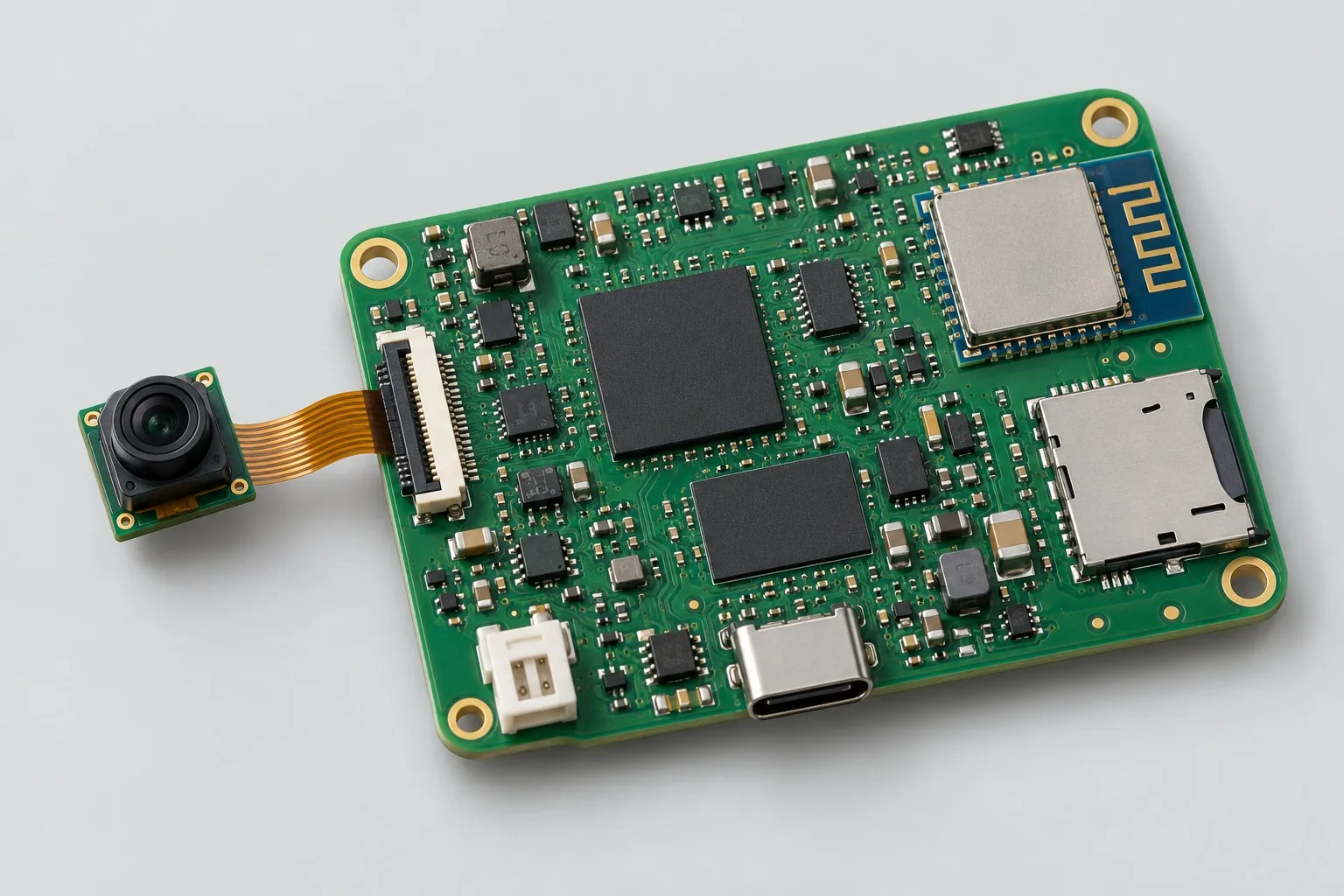
Can WiFi core boards be reused directly as video-recording mainboards?
Check camera interfaces, encoding, storage writing, and sustained throughput first; ordinary wireless access does not include complete recording paths. Network configuration and maintenance interfaces may be reusable, but assess processors and buffering separately for video tasks. Wireless MCU pin count does not establish video SoC capabilities.
How should I prepare an RFQ before commissioning WiFi/Bluetooth core board design?
Initially describe target functions, application, and existing files. Engineering quotations further confirm wireless protocols, data volume, and device count; board outline, enclosure-metal/antenna positions; selected module/IC models and Flash/PSRAM capacity. Provide editable schematics, PCB, and BOM for existing circuits, and revisions/reproduction records for faulty prototypes. List documentation gaps as review tasks so quotations do not use different assumptions.
How should WiFi/Bluetooth core board prototype validation costs be compared by operating condition?
Freeze prototype quantity, revision, equipment, and criteria sources first. For module/IC approaches, freeze throughput, model, antenna, and keepouts; compare space, debugging, and production tests. For wireless/power, freeze network type, reporting load, supply range, and reset strategy; run continuous transmission/reception and reconnection inside enclosures, capturing peak power responses. For upgrade recovery, freeze access, images, and rollback rules, interrupting download, write, and image switching separately. State whether raw data and issue closure are delivered; one power-on pass is not complete validation.
Compare related designs and plan the next step
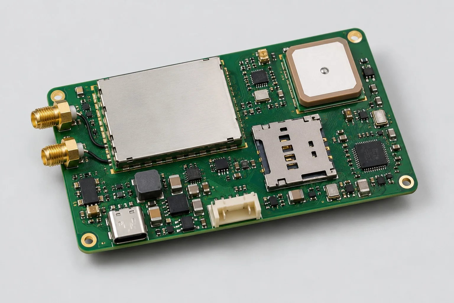
Compact 4G/Bluetooth/GPS tracker design · Pet video recorder core board design
Return HDI PCB design selection · Select solution by device function · Discuss your design requirements
Documentation Basis and Boundaries
Engineering reference | ESP32-S3 PCB layout: power, RF, and antenna clearance: the ESP32-S3 guide covers device power, USB, memory, and RF layout; confirm actual protocol functions against selected modules and software revisions.