Engineering reference design · prototype validation pending
Vibration acquisition board design: vibration inputs to dual ADCs and USB
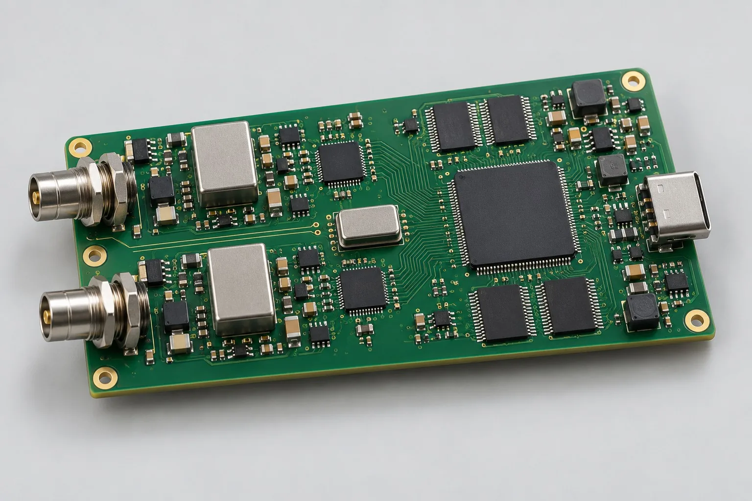
The dual-channel board sends two differential voltage inputs through anti-aliasing and synchronized ADCs, forming waveform records with common clocks, DMA buffers, and continuous USB upload. IEPE excitation is separate expansion; accept bandwidth, phase, and receiver pauses separately.
Custom development reference design. The parameters below are requirement configurations and design targets; validate product performance through agreed prototype tests.
| Functional Partition | Design and verification scope |
|---|---|
| Two-Channel Vibration Input | Define both input amplitudes, source impedances, and sensor bandwidths; IEPE versions add excitation/protection. |
| Wideband Filtering and ADC | Select differential drivers and ADS127L11-class ADCs by filter settings, checking frequency response, latency, and overload recovery. |
| Synchronous clock/buffer | Constrain both ADCs with common clocks/start synchronization; DMA/buffers retain frame sequence and timestamps. |
| USB Continuous Upload | Measure USB 2.0 HS payload throughput with actual hosts/drivers; mark buffer overflows during receiver pauses. |
| Analog/digital power supply | Partition 12V input into analog, digital, and USB domains; compare ripple, ground differences, and mating effects. |
| Trigger / data integrity | Use common-source signals for amplitude/phase and crosstalk, checking raw-file sequence, triggers, and dropped frames; rates cannot establish synchronization. |
How much does vibration acquisition board design cost, and how is it quoted?
Sensor inputs and continuous data paths jointly affect costs. Voltage inputs and IEPE excitation need different circuits; amplitude/phase and filter-delay requirements alter front ends/software. Separate conditioning/sampling, USB buffering/upload, sensor integration, and bandwidth validation rather than estimating by two ADC channels alone.
Quotation terms depend on the approved files, quantity, material supply, tests and delivery requirements.
Prepare a structured RFQ or use the short inquiry form.
| Quotation Items | What services are included | What to Check When Comparing Quotes |
|---|---|---|
| Circuit and PCB Design | Dual-channel analog conditioning/filtering, synchronization budget | Reusable portions of existing designs and circuit/mechanical changes |
| Software and Validation | Buffer and continuous USB upload | IEPE excitation/conditioning requires dedicated circuitry; ordinary voltage inputs are not direct IEPE inputs |
| Prototype Preparation | Bare PCB, BOM procurement, assembly, and agreed prototype quantity | Whether material/component revisions, prototype quantities, and test targets match |
| Subsequent Revision | Record new requirements separately from post-test corrections | How agreed changes, source files, and validation results are delivered |
How do vibration and low-speed process acquisition boards differ?
Vibration paths emphasize bandwidth, amplitude/phase, filter latency, and sustained throughput; slow process variables emphasize low-frequency errors. Channel count alone cannot justify reusing input types, ADCs, or filters.
Are higher vibration sampling rates always better?
Define target bands and amplitude/phase errors first, then select analog anti-aliasing/digital filtering. Higher rates add buffering, upload, and processing burdens and cannot replace matched sensors/front ends.
Does vibration board development include IEPE power?
IEPE excitation/conditioning requires dedicated circuitry; ordinary voltage inputs are not direct IEPE inputs. State whether sensor types, excitation, protection, and amplitude-frequency validation are included.
Reference configuration: vibration inputs to dual ADCs and USB
| Configuration Field | Reference Configurations/Selections | Basis and Status |
|---|---|---|
| Finished Product Function | Two-channel synchronized vibration/transient waveform acquisition | Design Objective |
| Input Configuration | 2 differential voltage inputs; IEPE excitation is separate expansion | Design Objective |
| Sampling Target | 200 kSPS per channel as an example target | Design Objective |
| ADC Candidate | Two ADS127L11-class ADCs | Design Objective |
| Resolution Specification | 24-bit encoding; no system ENOB claim | Design Objective |
| Analog Front End | Differential driver plus anti-aliasing filter | Design Objective |
| Synchronization Structure | Common clock + synchronization + timestamps | Design Objective |
| Transmission Interface | USB 2.0 HS target or Ethernet alternative | Design Objective |
| Buffer Configuration | MCU/FPGA DMA + external buffer | Design Objective |
| Power Target | 12V input; separate analog, digital, USB domains | Design Objective |
| Stackup Candidate | 6–8 layers; continuous ground references for clocks/high-speed traces | Design Objective |
| Test Interface | Reference clock, front-end input, ADC-output probes | Design Objective |
Filtering delay and continuous buffering
For broadband filter settings, focus on frequency response; for low-latency settings, focus on control latency. Filter settings become part of the revision configuration.
Dual-channel synchronization requires clocks, startup, and frames together; equal-length traces alone cannot establish synchronization accuracy.
Continuous rates include headers/timestamps; calculate buffer depth and worst-case USB scheduling gaps first.
Design budget and trade-off examples
Check design targets with engineering calculations
Two channels at 200kS/s each and 16bit produce 2×200000×2=800000B/s raw data; retaining 1 second requires at least 0.8MB payload storage.
Conditions and Scope of Application:This example assumes 16bit output packing; 24bit raw output needs 1.2MB/s payload. It excludes headers/buffer management and does not establish actual USB throughput. Test hosts, drivers, and write pauses for continuous acquisition.
Replace examples with selected components and record margins; calculations support design choices, while prototype records support acceptance.
Power and layout for vibration inputs to dual ADCs and USB
- Place analog drivers/filters near ADCs; keep clocks away from inputs and DC/DC inductors.
- Arrange differential input components symmetrically; probes must not create long branches.
- Keep USB traces off power-plane splits; evaluate low-parasitic protection candidates and connector transitions.
Vibration acquisition board development input
- Signal amplitudes, bandwidth, sensor outputs, IEPE need
- Synchronization tolerance, recording duration, host protocol
- Computer connection, isolation, ground-potential differences
If circuit files exist, provide editable schematics, PCB, BOM, and current issues, and agree on review or revision scope. If only functions are defined, freeze this page's inputs before selection and circuit development. Agree separately on control-software and external-application responsibilities, interfaces, and acceptance.
Vibration acquisition board phase delivery
| Stage | Engineering Work for This Proposal | Reviewable Deliverables |
|---|---|---|
| Requirements and Design Freeze | Freeze input/IEPE approaches, bandwidth, synchronization tolerance, duration, and host protocol | Functional/interface requirements, mechanical revision, acceptance conditions, and open items |
| Schematic and Component Selection | Design differential drivers, filters, dual ADCs, common clocks, DMA buffers, USB paths | Editable schematics, controlled BOM, footprint checks, and design calculations for these circuits |
| Layout and Routing | Implement symmetric analog layout, short clock loops, USB references, and controlled probes | PCB source files, actual stackup/hole/net constraints, DRC, and assembly-dimension checks |
| Simulation/Calculation | Analyze filter response/latency, clock skew, data packing, and receiver-pause buffering | Design calculations/models, input conditions, margins, and items awaiting measurement |
| Prototype and Software | Build dual-channel prototypes and integrate startup synchronization, triggers, timestamps, continuous upload | Fabrication package, dual-channel prototypes, agreed driver/upload firmware, frame formats, filters, and data-check tool instructions |
| Testing and Version Closure | Sweep amplitude/phase, common-source synchronization, and overload recovery; count dropped frames during continuous upload and after pauses | Procedures, wiring, raw results, and decisions for the prototype revision; include issue/change and limitation lists |
Dual-channel amplitude/phase and continuous upload verification
- Sine sweep to obtain amplitude and phase frequency response
- Measure channel phase difference and crosstalk for same-source signals
- Dropped frames/timestamp consistency during continuous raw-data upload
- Overload recovery, power interference, USB mating
Sweep amplitude/phase, common-source synchronization, and overload recovery; count dropped frames during continuous upload and after pauses. Record equipment, conditions, revisions, and criteria in reports, identifying passed and uncovered items.
Dual-channel amplitude/phase and continuous-upload validation worksheet
The table below turns vibration inputs to dual ADCs/USB into executable checks. Freeze samples, equipment, environment, and permitted deviations before execution; link results to this revision's raw records.
| Verification Object | Pre-Production Freeze | How to Test Prototypes in Practice | Delivery and Acceptance Records |
|---|---|---|---|
| Frequency Response and Phase | Sensor output, bandwidth, sample rate, amplitude/phase-error targets | Sweep common-source sine waves and test both channels separately | Deliver amplitude/frequency and phase/frequency curves, interchannel phase, calibration, and filter settings |
| Continuous Upload | Data format, USB mode, host configuration | Continuously sample/upload for agreed duration and simulate brief host pauses | Record dropped frames, sequences, buffer peaks, and recovery; sample rates do not establish sustained USB throughput |
| Overload Recovery | Rated input ranges, protection limits, permitted recovery duration | Apply input overload within approved bounds, then restore normal ranges | Retain recovery and protection-component temperature rise; identify differences between stimuli and actual sensors |
Manufacturing and assembly coordination for this design
- ADC/front-end resistor/capacitor package changes may alter parasitics; retest critical substitutions.
- Fixtures output synchronous signals; fabrication packages identify analog-clean regions and clock test points.
Link design revisions to schematics, BOM, PCB, fabrication, and software documentation. When fabricators adjust stackup, materials, or holes, or Assembly parties propose substitutions, recheck critical electrical and test conditions together.
Common questions on purchasing and customization
How much does vibration acquisition board design cost, and how is it quoted?
A project-specific quotation requires review of the available files, quantity, materials, requested tests, delivery destination, taxes, shipping, and trade terms. Complete development separately prices circuits, firmware, prototypes, and verification. Any formula on this page organizes cost inputs; it is not a quoted rate.View cost items, calculation conditions, and sources.
How to accept two-channel amplitude and phase vibration data?
Compare amplitude, phase, and filters frequency by frequency using identical sources/input conditions; retain raw data.
How to estimate buffer size for vibration recording length?
Define channel count, storage format, and continuous rate first, then add protocol/upload-pause margins rather than USB rated speed alone.
How should dual-channel vibration acquisition budgets validate critical risks first?
Review front ends using defined differential voltage inputs and target bands first, then validate ADCs, DMA buffers, and sustained USB data with a dual-channel 200kSPS example. List IEPE excitation, waveform software, and complete-sensor tests as separate options so basic voltage-acquisition and expanded sensor budgets can be compared independently.
Which constraints must customers provide for vibration-board routing only?
Provide both ADS127L11-class devices, common clocks, synchronization, analog drivers, and filters, defining USB/buffering approaches. Layout implements 6–8-layer returns/domains. Completed routing cannot replace acquisition development when analog bandwidth budgets and continuous-recording software remain incomplete.
Are USB upload and waveform analysis one software task?
Board firmware handles DMA, sequence, timestamps, and overflow; host software saves, displays, or analyzes spectra. State continuous raw-waveform disk recording, permitted interruptions, and analysis outputs. USB 2.0 HS rated speeds cannot replace actual long-duration recording tests.
Which filtering/synchronization settings should vibration acquisition source code include?
Retain ADC modes, clock/synchronization sequence, digital-filter latency, DMA lengths, and frame definitions. Link hardware to anti-aliasing/differential-driver revisions; deliver frequency-by-frequency amplitude/phase, raw samples, and dropped-sample logs so bandwidth changes can be assessed across the entire path.
How should adding IEPE to voltage inputs be requoted?
Add excitation sources, sensor-bias adaptation, protection, and conditioning, identifying cables/sensors. ADCs/buffers may remain, but revalidate bandwidth, noise, and amplitude/phase. Costs include circuits/tests rather than renaming interfaces IEPE.
Can dual-channel acquisition reuse low-speed eight-channel software?
Evaluate reusable frame/log tools, but redesign sustained rates, common clocks, and DMA queues for vibration tasks. Low-speed calibration cannot replace broadband amplitude/phase and anti-aliasing tests. List reusable modules first; fewer channels do not automatically mean simpler development.
How should I prepare an RFQ before commissioning vibration acquisition board design?
Initially describe target functions, application, and existing files. Engineering quotations further confirm amplitude, bandwidth, sensor outputs, and IEPE needs; synchronization, duration, and host protocols; computer connections, isolation, and ground differences. Provide editable schematics, PCB, and BOM for existing circuits, and revisions/reproduction records for faulty prototypes. List documentation gaps as review tasks so quotations do not use different assumptions.
How should vibration acquisition prototype validation costs be compared by operating condition?
Freeze prototype quantity, revision, equipment, and criteria sources first. For response/phase, freeze sensor outputs, bandwidth, rates, and errors; sweep common-source sines and test both channels. For continuous upload, freeze formats, USB, and hosts; sample/upload for agreed durations and simulate pauses. For overload recovery, freeze rated ranges, limits, and durations; apply approved overloads and return to normal ranges. State whether raw data and issue closure are delivered; one power-on pass is not complete validation.
Compare related designs and plan the next step
DDR storage interface motherboard design solution
Return to high-speed PCB design selection · Select solution by device function · Discuss your design requirements
Documentation Basis and Boundaries
Engineering reference | ADS127L11 Chinese-language device reference: selection conditions and board-level validation: ADS127L11 documentation references ADC filtering, synchronization, and interfaces; IEPE excitation, system bandwidth, and USB payload throughput need separate implementation.