Engineering reference design · prototype validation pending
5.8GHz PCB design: 5.8GHz through-path and filter evaluation
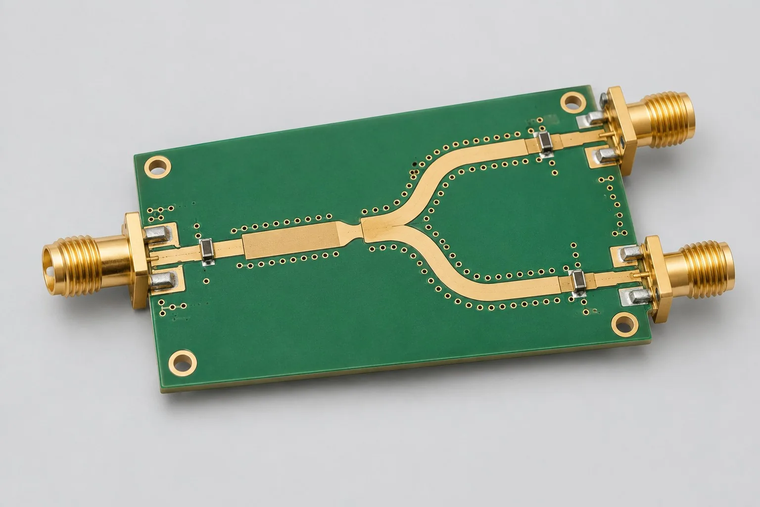
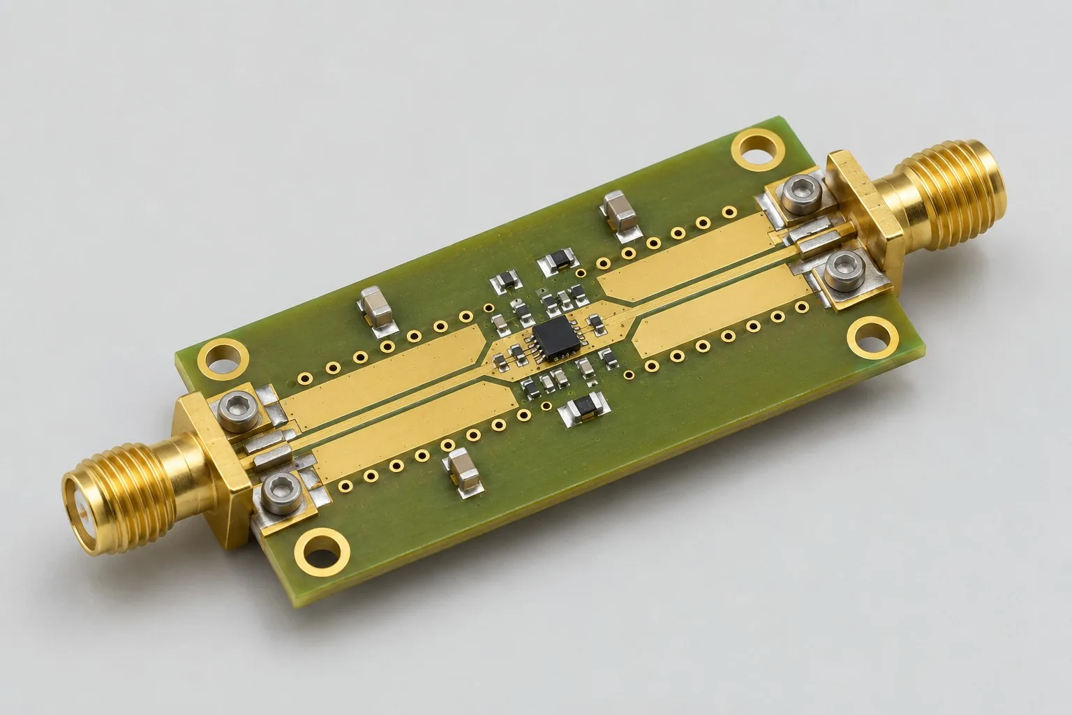
5.8GHz microwave evaluation boards compare passive through and filtered paths between SMA ports to assess materials, connector transitions, and board transmission loss. Optional gain extensions require separately selected in-band devices, delivering S-parameters at the same calibration plane.
Custom development reference design. The parameters below are requirement configurations and design targets; validate product performance through agreed prototype tests.
| Functional Partition | Design and verification scope |
|---|---|
| SMA Input Calibration Plane | Confirm input SMA models, board thickness, and calibration reference planes; handle cable/adapter losses separately. |
| Microwave Transition and Transmission Line | Design microwave transitions, transmission lines, and ground vias for actual materials/stackups; record dimensional tolerances. |
| Channel / Component Area | The base version compares through paths and inserted filters; active extensions require separate band, bias, and stability review. |
| SMA Output Calibration Plane | Maintain comparable output transitions; agree port calibration or de-embedding to board transmission-line sections. |
| Substrate and Ground Reference | Check frequency/test conditions, copper treatments, and continuous grounds for RO4350B-type materials; passive versions do not establish powered performance. |
| Fixture / S-parameters | Retain S11/S21, group delay, and calibration records; separately document connector reinstallation and sample repeatability. |
How much does 5.8 GHz microwave PCB design cost, and how is it quoted?
For 5.8GHz evaluation boards, first define passive through paths, filter comparisons, or active extensions. Port transitions, material models, and calibration planes determine simulation/measurement scope; active versions add devices and biasing. Separate structural design, comparison samples, measured S-parameters, and data delivery; one sample price does not represent complete evaluation costs.
Quotation terms depend on the approved files, quantity, material supply, tests and delivery requirements.
Prepare a structured RFQ or use the short inquiry form.
| Quotation Items | What services are included | What to Check When Comparing Quotes |
|---|---|---|
| Circuit and PCB Design | Microwave material and port transition modeling | Reusable portions of existing designs and circuit/mechanical changes |
| Software and Validation | Through/filtered prototype and S-parameter measurement | Agree models, connector reference planes, through/calibration structures, and measured S-parameters separately |
| Prototype Preparation | Bare PCB, BOM procurement, assembly, and agreed prototype quantity | Whether material/component revisions, prototype quantities, and test targets match |
| Subsequent Revision | Record new requirements separately from post-test corrections | How agreed changes, source files, and validation results are delivered |
Should 5.8GHz evaluation boards use passive channels or add gain stages?
Start with passive through/filter comparisons of material and port losses; add in-band devices and biasing when gain is needed. Design, power, and stability verification differ; passive-board quotations are not active-board budgets.
Should 5.8GHz boards use two-layer RF boards or hybrid multilayers?
Passive channels can compare two-layer continuous-ground structures. Consider hybrid stackups when also carrying control and complex power circuits. Align ports and target bands before comparing loss, structures, and fabrication costs.
Do microwave PCB design fees include network-analyzer testing?
Agree models, connector reference planes, through/calibration structures, and measured S-parameters separately. Confirm delivery of raw Touchstone and calibration records instead of only an insertion-loss screenshot.
Reference configuration for 5.8GHz through-path and filter evaluation
| Configuration Field | Reference Configurations/Selections | Basis and Status |
|---|---|---|
| Finished Product Function | Microwave transmission/filtering channel evaluation | Design Objective |
| Center Frequency Target | 5.8GHz requirement example; filter-defined passband | Design Objective |
| Port Configuration | SMA input/output each 1 channel | Design Objective |
| Channel Solution | Passive through-path baseline + inserted-filter comparison | Design Objective |
| Gain Extension | Gain stages require devices covering target bands | Design Objective |
| Material Candidate | RO4350B-type RF material or equivalent | Design Objective |
| Impedance Target | Single-ended 50 Ω; calculated by PCB fabricator stackup | Design Objective |
| Stackup Candidate | Compare a two-layer RF board with a four-layer hybrid stackup | Design Objective |
| Power Supply Option | Passive version unpowered; independent bias for active extensions | Design Objective |
| Reference plane | Connector end face or de-embedding to board trace | Design Objective |
| Calibration Structure | In-board direct path/calibration test strip option | Design Objective |
| Validation outputs | S11/S21, group delay, and manufacturing-deviation comparison | Design Objective |
Passive baseline and active extension
Fabricating a passive baseline first helps distinguish material/connector losses from active-component effects.
Hybrid stackups can reduce RF material use by placing control circuits on ordinary dielectrics, but add lamination and transition review.
Include filter-package parasitics and port transitions in electromagnetic models; whole-board measurements establish final passbands.
Design budget and trade-off examples
Check design targets with engineering calculations
If short-board S21 is −0.8dB and long-board response is −1.2dB under identical calibration, the difference is 0.4dB. Use this to estimate incremental-length loss only when transitions are comparable and de-embedding assumptions hold.
Conditions and Scope of Application:These hypothetical values illustrate analysis, not measured material data. Record frequency, calibration planes, fixtures, and repeatability.
Replace examples with selected components and record margins; calculations support design choices, while prototype records support acceptance.
Power and layout for 5.8GHz through-path and filter evaluation
- Arrange connectors, width transitions, and filters along straight paths; include ground gaps and via arrays in simulation.
- Record material-data test conditions separately from design dielectric parameters; one typical Dk does not cover every frequency.
- Match edge SMA ground pads to board thickness; reference strips use identical copper treatments and stackups to products.
Microwave evaluation board development input
- Passband width, insertion/return-loss targets, and connector models
- Acceptable materials, board thickness, copper foil, and surface finishes
- Network-analyzer bands, fixtures, and de-embedding methods
For existing circuits, provide editable schematics, PCB files, BOMs, and current issues, agreeing review/revision scope. For functional requirements alone, freeze this page's inputs before selection and circuit development. Define base-board ports, test wiring, and assembly scope; review added active/control circuits separately.
Microwave evaluation board phase delivery
| Stage | Engineering Work for This Proposal | Reviewable Deliverables |
|---|---|---|
| Requirements and Design Freeze | Freeze 5.8GHz passband, insertion/return loss, ports, and candidate materials | Functional/interface requirements, mechanical revision, acceptance conditions, and open items |
| Schematic and Component Selection | Design through/filter circuits and connector transitions; freeze active-extension devices/biasing separately | Editable schematics, controlled BOM, footprint checks, and design calculations for these circuits |
| Layout and Routing | Implement transmission lines, ground gaps/via fences, and port transitions; plan same-board calibration strips | PCB source files, actual stackup/hole/net constraints, DRC, and assembly-dimension checks |
| Simulation/Calculation | Build material/port electromagnetic models; compare in-band S-parameters and de-embedding sensitivity | Design calculations/models, input conditions, margins, and items awaiting measurement |
| Prototype and Software | Fabricate through/filter samples with port drawings, calibration configurations, and repeatable connection methods | Manufacturing package, through/filter evaluation samples, port/de-embedding drawings, calibration files, and Touchstone; active-extension documentation separately commissioned |
| Testing and Version Closure | Measure S-parameters/group delay; compare models, material samples, and repeated connector assembly | Procedures, wiring, raw results, and decisions for the prototype revision; include issue/change and limitation lists |
Microwave S-parameters and repeatability verification
- Measure calibrated S-parameters/group delay and retain raw Touchstone
- Compare through paths, filtered paths, and simulation deviations
- Impact of connector reassembly on results
- Compare insertion loss across material/copper-treatment samples
Measure S-parameters/group delay; compare models, material samples, and repeated connector assembly. Reports specify equipment, conditions, revisions, and criteria, recording passed and uncovered items.
Microwave S-parameter and repeatability verification worksheet
The table converts 5.8GHz through/filter evaluation into executable checks. Freeze samples, equipment, environments, and allowable deviations before execution; link results to this revision's raw records.
| Verification Object | Pre-Production Freeze | How to Test Prototypes in Practice | Delivery and Acceptance Records |
|---|---|---|---|
| Measurement Reference Plane | Operating bandwidth, port/fixture models, calibration, and de-embedding methods | Measure calibrated S-parameters/group delay on through/evaluation channels | Retain Touchstone, calibration records, and reference-plane drawings; exclude cable losses from board-level results |
| Model and Material | Materials/copper treatment, stackup, dielectric model, and target insertion loss | Compare simulation and identically conditioned sample measurements, identifying material lots | Deliver deviation bands and sensitive parameters; simulations are not factory measurements |
| Assembly Repeatability | Connector soldering, fastening, and permitted repeatability deviations | Repeat connector/cable removal and installation, then remeasure the same channel | Retain each curve and fastening condition to identify port-transition deviations |
Manufacturing and assembly coordination for this design
- The PCB fabricator confirms RF material lots, lamination structures, and copper-roughness definitions.
- SMA soldering/alignment fixtures control port transitions; fix measurement reference planes by revision.
Link design revisions to schematics, BOM, PCB, fabrication, and software documentation. When fabricators adjust stackup, materials, or holes, or Assembly parties propose substitutions, recheck critical electrical and test conditions together.
Common questions on purchasing and customization
How much does 5.8 GHz microwave PCB design cost, and how is it quoted?
A project-specific quotation requires review of the available files, quantity, materials, requested tests, delivery destination, taxes, shipping, and trade terms. Complete development separately prices circuits, firmware, prototypes, and verification. Any formula on this page organizes cost inputs; it is not a quoted rate.View cost items, calculation conditions, and sources.
Why must microwave evaluation quotations define calibration planes?
Different planes include different connectors/cables, making test costs and insertion losses incomparable. Align measurement objects before comparing prices.
What data needs to be delivered for microwave prototype?
Retain material/stackup revisions, port wiring, calibration records, and raw S-parameters for repeatable through/filter comparisons.
How can microwave evaluation budgets establish a baseline first?
First commission 5.8GHz passive through paths, port transitions, and same-board reference structures, then insert filters for comparisons at identical reference planes. Active gain requires separately selected in-band devices, biasing, and stability tests. Quote all three packages separately; obtain comparable losses before expansion so passive prices are not mistaken for active-system prices.
How are microwave Layout and electromagnetic-modeling charges separated?
Layout implements approved geometry, stackups, and SMA footprints. Port, filter, and material modeling handles structural design and analysis. Measured validation also needs calibration/de-embedding plans; routing 50Ω traces alone does not cover complete S11/S21 and group-delay evaluation.
Do passive 5.8GHz boards need control-software development?
Passive through/filter base versions are unpowered and should not incur forced firmware charges. Added switchable devices or gain-bias control require defined GPIO, states, and debug software. Agree analyzer acquisition/processing scripts separately from board firmware.
What reproducible data should microwave design source files include?
Agree actual materials/stackups, port geometry, simulation models/inputs, and same-board through/calibration structures. Deliver raw Touchstone, calibration, and de-embedding records, identifying connector faces or board trace sections. Screenshots alone cannot support later material/connector comparisons.
How should microwave design fees be reassessed after RF material changes?
Check Dk/Df frequency/measurement conditions, actual thickness, copper, and fabrication tolerances; recalculate widths and filter geometry. Unchanged outlines do not mean unchanged electrical lengths. Separate model updates, geometric changes, and same-reference-plane sample measurements, beyond material price differences.
Can microwave through structures be reused on RF gain boards?
Assess connector/reference-structure reuse by band, but active paths add matching, low-noise bias, thermal design, and stability. A 900MHz front-end reference device does not automatically cover 5.8GHz; reuse requires documented target-band support.
How should quotation documentation be prepared for 5.8 GHz microwave PCB design?
Initially describe functions, applications, and available files. Engineering quotations further confirm passband width, insertion/return-loss targets, connector models, acceptable materials/thickness/copper/finishes, analyzer bands, fixtures, and de-embedding. Provide editable schematics, PCB files, and BOMs for existing designs, or revisions/reproduction records for faulty prototypes. List gaps as review tasks to prevent differing assumptions.
How should 5.8GHz microwave PCB prototype verification costs be compared by operating condition?
Fix prototype quantities, revisions, equipment, and criteria sources. Separately review measurement planes: freeze bandwidth, ports/fixtures, calibration/de-embedding, then measure calibrated through/evaluation S-parameters and group delay. Models/materials: freeze materials/copper treatments, stackups, dielectric models, and insertion-loss targets; compare simulation with identically conditioned samples, identifying lots. Assembly repeatability: freeze connector soldering/fastening and allowable deviations; repeatedly reconnect connectors/cables and remeasure. Specify raw-data and issue-closure deliverables; DC continuity alone does not verify the passive RF path.
Compare related designs and plan the next step
2.4GHz antenna feed and power-divider board design
Return to high-frequency PCB design selection · Select solution by device function · Discuss your design requirements
Documentation Basis and Boundaries
Engineering reference | RO4350B material: high-frequency parameters and stackup confirmation: Rogers documentation supports selected-material electrical/fabrication conditions, not filter or gain-stage bands/performance.