Engineering reference design · prototype validation pending
50-ohm PCB design: module-to-antenna 50Ω interconnects
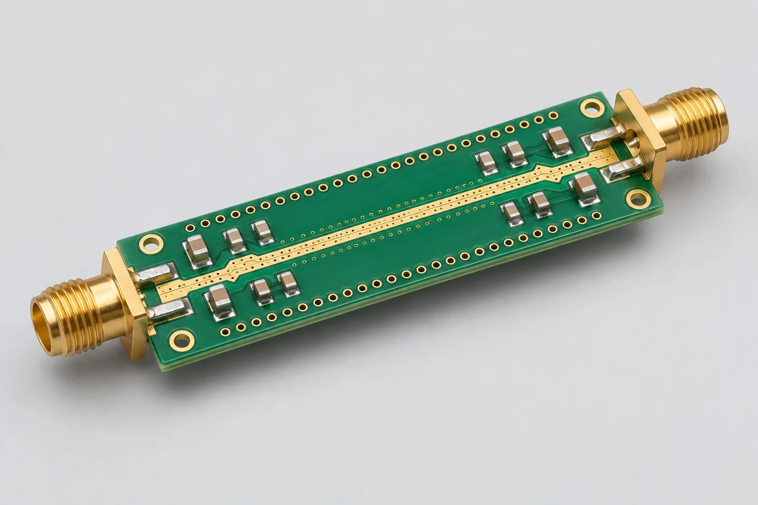
50Ω RF interface boards connect radio modules, antennas, or instruments using microstrip/coplanar waveguides and compact matching provisions. Agree loss, reflection, and reconnection results against actual bands, fabricator stackups, and port calibration planes.
Custom development reference design. The parameters below are requirement configurations and design targets; validate product performance through agreed prototype tests.
| Functional Partition | Design and verification scope |
|---|---|
| SMA RF Ports | Freeze SMA/module-pad ports, compatible thickness, and reference planes; exclude adapter loss from onboard feedlines. |
| 50 Ω candidate transmission line | Calculate 50Ω microstrip/coplanar waveguides using actual dielectrics, copper weight, and ground structures; define tolerances by order/test method. |
| Matching/adjustable network | Keep π-tuning positions compact, model unpopulated-pad parasitics, and issue controlled matching BOMs after tuning. |
| RF Output Port | Select output antenna connectors/SMA by system connections; review coaxial cables/enclosure fastening together. |
| Layer Stack and Ground Reference | Maintain continuous ground under RF; review vias, copper treatment, and edges together. Passive interconnects need no supply. |
| Calibration / Reflection Test | Measure S-parameters/necessary TDR at specified planes; use reconnection/soldering samples to distinguish line/port deviations. |
How much does 50Ω RF PCB design cost, and how is it quoted?
For 50Ω RF board quotations, define RF ports/reference planes. Stackup-based transmission-line design differs in cost from connector transitions, material comparisons, and whole-board reflection measurements. Align microstrip/coplanar structures, lengths, and fixtures in comparisons; fabricator-coupon costs do not replace whole-board port measurements.
Quotation terms depend on the approved files, quantity, material supply, tests and delivery requirements.
Prepare a structured RFQ or use the short inquiry form.
| Quotation Items | What services are included | What to Check When Comparing Quotes |
|---|---|---|
| Circuit and PCB Design | RF stackups, microstrip/coplanar structures, and connectors | Reusable portions of existing designs and circuit/mechanical changes |
| Software and Validation | Reflection and connection repeatability | Coupons verify corresponding transmission structures; product ports also include connectors/transitions |
| Prototype Preparation | Bare PCB, BOM procurement, assembly, and agreed prototype quantity | Whether material/component revisions, prototype quantities, and test targets match |
| Subsequent Revision | Record new requirements separately from post-test corrections | How agreed changes, source files, and validation results are delivered |
Should 50Ω RF lines use microstrip or coplanar waveguides?
Compare thickness, port transitions, ground structures, and available width. Both require actual stackups/surroundings in calculations; do not transfer widths directly between structures.
Can 50Ω boards become 75Ω boards by changing impedance labels alone?
No. Transmission structures, connectors, sources, and loads must match the system. Recalculate dimensions and reverify ports after target changes instead of merely editing fabrication notes.
Do coupons in 50Ω PCB quotations represent actual ports?
Coupons verify corresponding transmission structures; product ports also include connectors/transitions. Itemize fabricator impedance checks separately from whole-board RF measurements to avoid mixing results.
Reference configuration for module-to-antenna 50Ω interconnects
| Configuration Field | Reference Configurations/Selections | Basis and Status |
|---|---|---|
| Finished Product Function | RF interconnect from module to antenna/instrument | Design Objective |
| Band Target | 100MHz–3GHz requirement example | Design Objective |
| Impedance Target | Single-ended 50Ω; tolerance defined by order/test method | Design Objective |
| Port Configuration | SMA input/output or module pads → IPEX | Design Objective |
| Channel Structure | Microstrip/coplanar waveguide two candidates | Design Objective |
| Material Selection | Compare FR-4 and RF dielectrics against loss budgets | Design Objective |
| Stackup Candidate | Two or four layers with a continuous ground reference beneath RF traces | Design Objective |
| Connector Boundary | connector model and applicable board thickness frozen first | Design Objective |
| Matching Reserve | π-matching positions; revision-controlled BOM after tuning | Design Objective |
| Power Supply Requirement | Passive basic version requires no power | Design Objective |
| Calibration method | Port calibration plus in-board direct path reference | Design Objective |
| Validation outputs | TDR/impedance, S-parameters, and assembly repeatability | Design Objective |
Microstrip and Coplanar Waveguide Routing
Short paths can be evaluated with conventional substrates; compare high-frequency dielectrics for longer paths or stricter loss requirements.
Coplanar ground spacing and via arrays are structural parameters too; signal width alone is insufficient.
Fix connector reference planes to compare simulations, coupons, and actual boards.
Design budget and trade-off examples
Check design targets with engineering calculations
For port voltage-reflection magnitude 0.1, return loss RL=−20log10(0.1)=20dB, and standing-wave ratio is (1+0.1)/(1−0.1)≈1.22.
Conditions and Scope of Application:This illustrates metric conversion only. Match frequency, reference planes, and fixtures; DC continuity cannot establish RF matching.
Replace examples with selected components and record margins; calculations support design choices, while prototype records support acceptance.
Power and layout for module-to-antenna 50Ω interconnects
- Avoid long RF stubs/unnecessary layer changes; implement port-pad transitions.
- Keep π-matching positions compact; model reserved unpopulated-pad parasitics.
- Distribute ground vias along feedlines and around ports; review copper treatments and edge clearances.
RF Interface Board R&D Input
- Bands, allowable insertion/return loss, and feedline lengths
- Connector/antenna-connector models and actual fabricator stackups
- Instrument calibration, reference planes, and temperature conditions
For existing circuits, provide editable schematics, PCB files, BOMs, and current issues, agreeing review/revision scope. For functional requirements alone, freeze this page's inputs before selection and circuit development. Define base-board ports, test wiring, and assembly scope; review added active/control circuits separately.
RF Interface Board Phase Delivery
| Stage | Engineering Work for This Proposal | Reviewable Deliverables |
|---|---|---|
| Requirements and Design Freeze | Freeze bands, lengths, loss/return loss, ports, and test planes | Functional/interface requirements, mechanical revision, acceptance conditions, and open items |
| Schematic and Component Selection | Define passive ports, π-matching networks, and connector footprints | Editable schematics, controlled BOM, footprint checks, and design calculations for these circuits |
| Layout and Routing | Implement controlled feedlines, port transitions, and ground fences; minimize stubs/layer changes | PCB source files, actual stackup/hole/net constraints, DRC, and assembly-dimension checks |
| Simulation/Calculation | Calculate impedance from approved stackups; analyze connector/matching-pad parasitics and losses | Design calculations/models, input conditions, margins, and items awaiting measurement |
| Prototype and Software | Fabricate RF interconnect samples with fixed calibration, torque, and soldering-position configurations | Manufacturing package, passive interface samples, stackup/impedance inputs, port/calibration drawings, matching BOMs, and Touchstone |
| Testing and Version Closure | Retain S11/S21 and time-domain responses; compare coupons, models, and repeated assembly | Procedures, wiring, raw results, and decisions for the prototype revision; include issue/change and limitation lists |
RF reflection and connection repeatability verification
- Measure S11/S21 at specified planes and retain files
- Locate port/via discontinuities using impedance/time-domain responses
- Different soldering samples and reconnection repeatability
- Out-of-band response and stability after temperature changes
Retain S11/S21 and time-domain responses; compare coupons, models, and repeated assembly. Reports specify equipment, conditions, revisions, and criteria, recording passed and uncovered items.
RF reflection and connection-repeatability verification worksheet
The table converts module-to-antenna 50Ω interconnects into executable checks. Freeze samples, equipment, environments, and allowable deviations before execution; link results to this revision's raw records.
| Verification Object | Pre-Production Freeze | How to Test Prototypes in Practice | Delivery and Acceptance Records |
|---|---|---|---|
| Reference Plane and Loss | Bands, impedance targets, port models, and de-embedding methods | Measure S11/S21 at specified planes; inspect time-domain discontinuities when necessary | Retain raw files/port drawings, distinguishing line, connector, and fixture contributions |
| Layer Stack Manufacturability | Actual materials, copper weight, dielectric thickness, and tolerances | Recalculate feedlines after fabricator stackup confirmation; compare coupon/sample results | Deliver calculation inputs and measured comparisons; do not copy another fabricator's widths |
| Soldering Reproducibility | Connector processes, torque, and repeatability specifications | Remeasure the same band across samples or repeated reconnections | Retain overlaid curves/sample revisions to locate joint and port-transition differences |
Manufacturing and assembly coordination for this design
- Keep width etch compensation, dielectric thickness, and copper-weight revisions consistent.
- Connector soldering angles and enclosure fastening affect ports; assembly drawings specify positioning methods.
Link design revisions to schematics, BOM, PCB, fabrication, and software documentation. When fabricators adjust stackup, materials, or holes, or Assembly parties propose substitutions, recheck critical electrical and test conditions together.
Common questions on purchasing and customization
How much does 50Ω RF PCB design cost, and how is it quoted?
A project-specific quotation requires review of the available files, quantity, materials, requested tests, delivery destination, taxes, shipping, and trade terms. Complete development separately prices circuits, firmware, prototypes, and verification. Any formula on this page organizes cost inputs; it is not a quoted rate.View cost items, calculation conditions, and sources.
Do RF boards need revision when SMA connectors change?
Envelopes, thickness matching, and transitions may change. Review pads/grounding before reflection measurements, beyond connector names.
How should RF transmission losses be compared across suppliers?
Align bands, lengths, materials, and connector reference planes; retain raw measurements/calibration conditions. Do not directly compare results including different cables.
How should RF interconnect budgets be divided by test object?
Freeze the 100MHz–3GHz requirement range, length, and SMA or module-to-IPEX ports, then separate stackup/transmission-line design, connector transitions, and whole-board measurements. Itemize fabricator coupons and actual-port S-parameters so routing-only prices are distinguishable from calibrated-measurement scope.
How should 50Ω width calculations and RF Layout be commissioned?
Calculations need actual materials, dielectrics, copper weight, and microstrip/coplanar selection. Layout also implements surrounding grounds, return vias, connectors, and π-matching positions. Approved customer structures permit routing-only scope; undefined structures add calculation/port review. No universal width fits all fabricators.
Do passive RF interconnects require software delivery?
Passive base versions need no onboard firmware. Instrument acquisition, calibration, or processing scripts may be agreed, specifying runtime equipment/results. Module-side communication control is system software, not automatically part of 50Ω interconnect PCB design.
What measurement boundaries should RF PCB sources retain?
Retain port models, thickness, transitions, matching BOMs, actual stackups, and TDR/S-parameter reference planes. Reports include raw data, calibration, and reconnection records so later connector changes can distinguish line versus port effects.
What work is added when microstrip changes to coplanar waveguide?
Recalculate widths, ground gaps, via fences, and port transitions; check available width/tolerances. With unchanged outlines, assess original connector reuse. Remeasure new structures; do not transfer microstrip coupon results directly.
Can one 50Ω interconnect be reused with any RF module?
Check module pads, bands, output conditions, and connectors. Identical 50Ω targets do not establish equal transitions/losses. Itemize reusable intermediate transmission structures; reconfirm module matching and actual-port measurements. Impedance names alone do not establish universality.
How should quotation documentation be prepared for 50Ω RF PCB design?
Initially describe functions, applications, and files. Engineering quotations further confirm bands, allowable insertion/return loss, lengths, connector/antenna models, actual stackups, calibration, reference planes, and temperatures. Provide editable schematics, PCB files, and BOMs for existing designs, or revisions/reproduction records for faulty prototypes. List gaps as review tasks to prevent differing assumptions.
How should 50Ω RF PCB prototype verification costs be compared by operating condition?
Fix prototype quantities, revisions, equipment, and criteria sources. Separately review planes/loss: freeze bands, impedance, ports, and de-embedding; measure S11/S21 and necessary time-domain discontinuities. Stackup manufacturability: freeze materials, copper, dielectrics, and tolerances; recalculate after fabricator confirmation and compare coupons/samples. Soldering repeatability: freeze processes, torque, and criteria; remeasure bands across samples/reconnections. Specify raw-data and issue-closure deliverables; DC continuity alone does not verify the passive RF path.
Compare related designs and plan the next step
USB high-speed differential interface board design
Return impedance control PCB design selection · Select solution by device function · Discuss your design requirements
Documentation Basis and Boundaries
Engineering reference | RO4350B material: high-frequency parameters and stackup confirmation: Rogers documentation applies only to corresponding materials; confirm 50Ω cross-sections, connectors, and tuned matching using actual stackups/port models.