Engineering reference design · prototype validation pending
DDR PCB design: controller to DDR memory
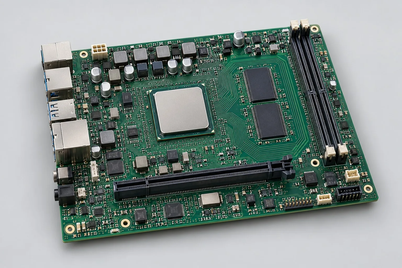
DDR mainboard design equips processors/FPGAs with external memory, boot storage, and debug interfaces. Start with customer-selected controllers/packages and constrain DQ/DQS, address/command, and clocks separately, delivering topology, timing budgets, and training validation.
Custom development reference design. The parameters below are requirement configurations and design targets; validate product performance through agreed prototype tests.
| Functional Partition | Design and verification scope |
|---|---|
| DDR Controller | Freeze SoC/FPGA, memory generation, bus width, and supported speed grades; confirm controller pins and initialization responsibility. |
| Topology/package constraints | Choose point-to-point/multidevice topology by controller guides, checking package delays, IBIS, and vias. |
| DDR Memory | DDR3L x16 and 256MB are requirement examples only; freeze BOMs after confirming part/voltage/density combinations. |
| Training and Application Loads | Actual controllers run training, address/random patterns, and sustained reads/writes; logs identify board and software settings. |
| Multi-Rail Power and Decoupling | Design DDR power, VREF, and termination by controller/memory architecture; capture supply/reference voltages during bursts. |
| Clock / SI and PI | Analyze timing, reflections, and supply noise separately, identifying missing models and risks requiring prototype closure. |
How much does high-speed DDR PCB design cost, and how is it quoted?
Distinguish routing to existing constraints from establishing and validating controller constraints. Model preparation, stackup review, timing analysis, and training-fault diagnosis are separate tasks. Schematics without software/models do not support layout-only budgets; list prototype and long-duration read/write targets/conditions too.
Quotation terms depend on the approved files, quantity, material supply, tests and delivery requirements.
Prepare a structured RFQ or use the short inquiry form.
| Quotation Items | What services are included | What to Check When Comparing Quotes |
|---|---|---|
| Circuit and PCB Design | Controller/DDR topology constraints, stackup, and model checks | Reusable portions of existing designs and circuit/mechanical changes |
| Software and Validation | Training logs and long-duration read/write verification | PCB sources and DDR initialization/training parameters are separate deliverables |
| Prototype Preparation | Bare PCB, BOM procurement, assembly, and agreed prototype quantity | Whether material/component revisions, prototype quantities, and test targets match |
| Subsequent Revision | Record new requirements separately from post-test corrections | How agreed changes, source files, and validation results are delivered |
How does DDR length matching alone differ from complete high-speed design?
Length matching is only part of routing constraints. Complete work checks supported topology, timing, returns, power, and initialization. Confirm model analysis, training, and read/write validation in quotations.
How should DDR layer count be selected, and can two layers be removed?
Arrange buses, references, and power by controller guides. Reducing layers matters only if breakout, returns, and power still meet constraints; lower bare PCB prices do not justify removing required reference layers.
Does DDR layout pricing include boot-software debugging?
PCB sources and DDR initialization/training parameters are separate deliverables. With existing software, agree on log analysis and revision regression; starting from scratch requires initialization and stress tests in scope.
Reference configuration: controller to DDR memory
| Configuration Field | Reference Configurations/Selections | Basis and Status |
|---|---|---|
| Finished Product Function | Processor/FPGA external-memory expansion | Design Objective |
| Storage Target | 1 DDR3L x16 group as a requirement example | Design Objective |
| Capacity Reference | 256MB target, determined by component-density combination | Design Objective |
| Operating Speed | Set by controller speed support and SI budget; no board-limit commitment | Design Objective |
| Main Controller Input | Customer-selected SoC/FPGA, package, pin constraints | Design Objective |
| Power domain | DDR voltage, termination/VREF by device architecture | Design Objective |
| External Interface | Debug UART, JTAG, boot storage | Design Objective |
| Stackup Candidate | 8 layer; DDR adjacent to reference ground | Design Objective |
| Topology Constraint | Separate address/command, clock, and data groups | Design Objective |
| Component Selection | Same-generation DDR, controller IBIS, and package models | Design Objective |
| Software Scope | Boot initialization, memory training, stress tests | Design Objective |
| Manufacturing Verification | Impedance coupons, netlists, package-breakout checks | Design Objective |
DDR topology and training boundary
First establish the controller, memory generation, and bus width, then select point-to-point or an applicable multidevice topology.
Added layers first address references, breakout, and power distribution; serpentine matching cannot fix wrong topology or drive configuration.
When models are incomplete, document simulation confidence and gaps; manufacturable routing review can still proceed.
Design budget and trade-off examples
Check design targets with engineering calculations
At 800MT/s, the unit interval UI=1/800MHz=1.25ns; subtract device, jitter, skew, and interconnect effects from available timing windows.
Conditions and Scope of Application:This example defines neither a specific DDR speed nor length-matching tolerance; use selected-controller manufacturer guides and package/board models.
Replace examples with selected components and record margins; calculations support design choices, while prototype records support acceptance.
Power and layout for controller-to-DDR memory
- Arrange DQS/DQ by byte groups, with separate clock/address-command constraints rather than one length rule for all nets.
- Review reference transitions and return vias at high-speed layer changes; include via stubs in SI budgets.
- Isolate VREF from switching noise and decouple locally; review DDR supply transients and returns together.
DDR mainboard development input
- Controller hardware guide, memory datasheet, IBIS models
- Target clock grade, topology, packages, temperature requirements
- Boot-software source, board outline, cooling, power budget
If circuit files exist, provide editable schematics, PCB, BOM, and current issues, and agree on review or revision scope. If only functions are defined, freeze this page's inputs before selection and circuit development. Agree separately on control-software and external-application responsibilities, interfaces, and acceptance.
DDR mainboard phase delivery
| Stage | Engineering Work for This Proposal | Reviewable Deliverables |
|---|---|---|
| Requirements and Design Freeze | Freeze controller/DDR parts, capacity, grades, models, and boot-software source | Functional/interface requirements, mechanical revision, acceptance conditions, and open items |
| Schematic and Component Selection | Complete memory topology, power/termination/VREF, boot/debug circuits | Editable schematics, controlled BOM, footprint checks, and design calculations for these circuits |
| Layout and Routing | Implement DQ/DQS byte-group constraints; check address/command, clocks, breakout, and return transitions | PCB source files, actual stackup/hole/net constraints, DRC, and assembly-dimension checks |
| Simulation/Calculation | Analyze SI/PI/timing with actual models, listing unmodeled packages/interconnects | Design calculations/models, input conditions, margins, and items awaiting measurement |
| Prototype and Software | Build mainboard prototypes and integrate initialization, training, and stress programs | Fabrication package, DDR prototypes, agreed initialization/training software, constraint reports, stress tests, and recovery instructions |
| Testing and Version Closure | Repeat cold/hot starts and continuous reads/writes, recording training parameters, memory errors, and power integrity | Procedures, wiring, raw results, and decisions for the prototype revision; include issue/change and limitation lists |
DDR training and read/write stress verification
- Pre-/post-layout simulation of timing/reflection risks
- Training records across voltage/temperature conditions
- Random/address-pattern and sustained read/write stress tests
- Measure supply ripple and write-burst voltage drops
Repeat cold/hot starts and continuous reads/writes, recording training parameters, memory errors, and power integrity. Record equipment, conditions, revisions, and criteria in reports, identifying passed and uncovered items.
DDR training and read/write stress validation worksheet
The table below turns controller-to-DDR memory into executable checks. Freeze samples, equipment, environment, and permitted deviations before execution; link results to this revision's raw records.
| Verification Object | Pre-Production Freeze | How to Test Prototypes in Practice | Delivery and Acceptance Records |
|---|---|---|---|
| Constraint Closure | Controller/DDR parts, speed grades, package models, topology | Review DQ/DQS byte groups, address/command, clocks, and layer-transition returns separately | Deliver constraint/routing reports, model revisions, and unmodeled items; all-net length matching is not the complete criterion |
| Training Stability | Operating voltage/temperature, training program, permitted-error definitions | Repeat startup/training across conditions and run address/random patterns and sustained reads/writes | Retain training parameters, failure counts, and memory-error logs, identifying firmware/board revisions each time |
| Power Supply Integrity | DDR power, VREF, termination, load-switching conditions | Measure supply/reference voltages during read/write bursts and compare with models | Retain probe locations, bandwidth, and power waveforms; confirm termination against this controller's guide |
Manufacturing and assembly coordination for this design
- Recalculate stackups using fabricator-provided dielectric/copper parameters; do not copy another factory's trace widths.
- Confirm coupon positions before design freeze; agree on critical BGA solder-joint inspection in the assembly plan.
Link design revisions to schematics, BOM, PCB, fabrication, and software documentation. Recheck critical electrical and test conditions when fabricators adjust stackup, materials, or holes or assemblers propose substitutes.
Common questions on purchasing and customization
How much does high-speed DDR PCB design cost, and how is it quoted?
A project-specific quotation requires review of the available files, quantity, materials, requested tests, delivery destination, taxes, shipping, and trade terms. Any formula on this page organizes cost inputs; it is not a quoted rate.View cost items, calculation conditions, and sources.
What should DDR prototype acceptance records include?
Freeze controller, memory, stackup, and initialization revisions; retain training logs, stress-test conditions, and errors.
Can DDR substitutions retain the original layout?
Check packages, controller support, and topology constraints before deciding; equal nominal capacities do not establish reusable layout/training parameters.
Is DDR constraint review or immediate routing more economical?
If controller model, DDR3L x16 example, packages, or initialization are undefined, review support and topology first. Commission eight-layer layout after usable constraints exist; separate modeling, training debug, and read/write stress tests to avoid discovering unsupported component/pin combinations after routing.
Which inspectable constraints should DDR layout quotations include?
Require separate topology, permitted skew, reference planes, and via rules for address/command, clocks, and data groups, checking VREF/termination too. Identify controller/memory revisions as constraint sources; one all-net length screenshot cannot represent complete high-speed routing.
Does customer-provided boot code eliminate training debugging?
Existing code reduces boot-environment setup, but check initialization for current controllers, DDR, and new stackups. Training logs/stress tests remain new-board validation; an old board booting does not establish new-board extended read/write or boundary reliability.
How should DDR model and source-file delivery be specified?
Agree on revisions and deliverable scope for PCB/schematics, grouped constraints, stackup, IBIS, and package models. Explain alternative evidence for licensed models; include training/initialization settings in software and unmodeled exclusions in reports. Simulation images do not replace traceable inputs.
Which limitations belong in layout-only quotations when DDR models are unavailable?
List available/missing controller, DDR3L, package/IBIS models and retain approved topology/constraint sources. Separate layout execution from model analysis. Agree on supplemental measurements/training/stress tests for missing models; do not label unanalyzed paths validated or independently promise operating rates.
Can existing DDR3L boards upgrade directly to another DDR generation?
The DDR name does not establish interface compatibility. Recheck generation voltage, timing, topology, and controller support. State retention conditions for reusable mechanics/debug tools; develop buses/initialization for new devices rather than treating substitution prices as generation-upgrade budgets.
How should I prepare an RFQ before commissioning high-speed DDR PCB design?
Initially describe target functions, application, and existing files. Engineering quotations further confirm controller guides, memory datasheets, and IBIS; clock grades, topology, packages, and temperatures; boot-software sources, outlines, cooling, and power budgets. Provide editable schematics, PCB, and BOM for existing circuits, and revisions/reproduction records for faulty prototypes. List documentation gaps as review tasks so quotations do not use different assumptions.
How should high-speed DDR prototype validation costs be compared by operating condition?
Freeze prototype quantity, revision, equipment, and criteria sources first. For constraints, freeze parts, speed grades, packages, and topology; review DQ/DQS, address/command, clocks, and transition returns. For training stability, freeze voltage/temperature, programs, and errors, then repeat startup/training and address/random/sustained tests. For power integrity, freeze supplies, VREF, termination, and load changes; measure burst supply/reference voltages and compare models. State whether raw data and issue closure are delivered; one power-on pass is not complete validation.
Compare related designs and plan the next step
Dual-channel broadband vibration acquisition board design
Return to high-speed PCB design selection · Select solution by device function · Discuss your design requirements
Documentation Basis and Boundaries
Engineering reference | AM437x DDR3 reference design: stackup, timing, and validation: TIDEP0012 addresses specific AM437x DDR layouts; VTT-free approaches do not apply universally to SoC/FPGA devices. Follow selected-controller guides.
TI's reference design addresses specific AM437x layout conditions; VTT-free termination does not apply directly to every SoC/FPGA here. Confirm controller, topology, and termination against each hardware guide.