Engineering reference design · prototype validation pending
RF gain-board design: front-end gain and bias
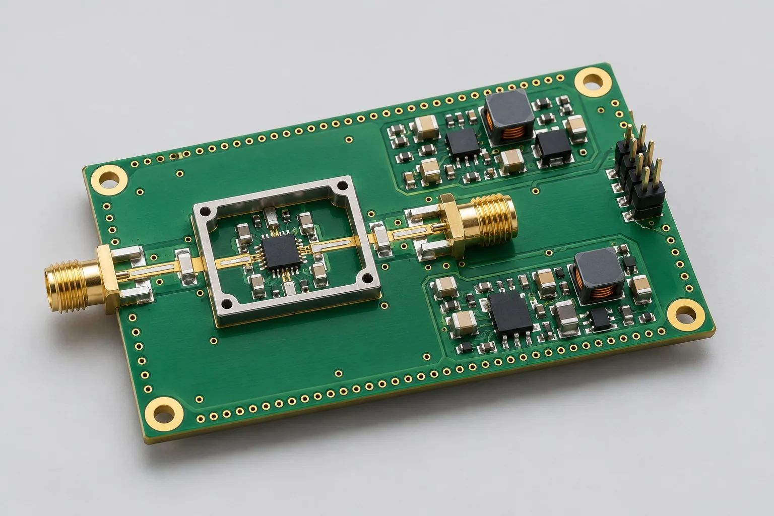
RF gain/bias boards provide front-end amplification, low-noise bias, and measurable RF ports for transceiver chains. ADL5602-type gain blocks are selection references; determine operating points by bands, input levels, and modulation. Higher output requires separate power-stage review.
Custom development reference design. The following parameters are requirement configurations and design targets; validate functions and performance through agreed prototype tests.
| Functional Partition | Design and verification scope |
|---|---|
| RF Input Match | Freeze input bands, levels, and source impedance; design matching/necessary limiting and record input measurement planes. |
| Gain / Amplifier stage | Check bandwidth, bias, gain, and compression for selected devices; typical device values are not whole-board guarantees. |
| Output Matching and Ports | Review output matching with downstream loads; include connector/feedline losses in actual output budgets. |
| Control/enable interface | GPIO enable and current/temperature readback are optional; define power-up, shutdown, and default fault states. |
| Low-Noise Bias Power Supply | Provide bias, current measurement points, and local decoupling in the 5V low-noise domain; record startup and supply boundaries. |
| Stability and Thermal Protection | Measure oscillation, compression/distortion, and recovery across approved loads, temperatures, and input ranges, linked to thermal structures. |
How much does RF gain-board design cost, and how is it quoted?
Start with bands, operating levels, and device approaches. Reference-circuit layout differs from matching, bias, compression, and stability development. Higher-output power stages and thermal provisions are not automatically included. Compare front-end development, sample components, and agreed RF measurement charges separately.
Quotation terms depend on the approved files, quantity, material supply, tests and delivery requirements.
Prepare a structured RFQ or use the short inquiry form.
| Quotation Items | What services are included | What to Check When Comparing Quotes |
|---|---|---|
| Circuit and PCB Design | RF gain devices, bias, and matching | Reusable portions of existing designs and circuit/mechanical changes |
| Software and Validation | Gain compression and stability check | Itemize device selection, matching BOMs, bias conditions, band measurements, and sample regression |
| Prototype Preparation | Bare PCB, BOM procurement, assembly, and agreed prototype quantity | Whether material/component revisions, prototype quantities, and test targets match |
| Subsequent Revision | Record new requirements separately from post-test corrections | How agreed changes, source files, and validation results are delivered |
How do RF gain boards differ from passive microwave boards?
Passive boards compare transmission/filter losses; gain boards add active devices, bias, power, and stability. Select by input levels, bands, and output conditions, beyond gain alone.
Is higher RF gain always better?
High gain must also suit input dynamic range, noise, compression, and stability. Define signal chains and operating levels before stages/bias to avoid sacrificing linear range for gain.
Do gain-board development fees include matching adjustment and RF tests?
Itemize device selection, matching BOMs, bias conditions, band measurements, and sample regression. Reference-circuit layout quotations do not cover completed board-level gain verification.
Reference configuration for RF front-end gain and bias
| Configuration Field | Reference Configurations/Selections | Basis and Status |
|---|---|---|
| Reference application | RF front-end gain and bias for the stated signal conditions | Illustrative configuration; prototype validation required |
| Finished Product Function | RF gain, bias control, measurement access | Design Objective |
| Band Reference | 900MHz requirement example; check device coverage | Design Objective |
| Component Candidate | ADL5602-type gain block as front-end reference | Design Objective |
| Port Target | 50Ω inputs/outputs, SMA debug interfaces | Design Objective |
| Power Supply Configuration | 5V low-noise domain; bias enable/current measurement points | Design Objective |
| Output Boundary | Separate system-power targets; typical device values are not guarantees | Design Objective |
| Stackup Candidate | 4 layer FR-4 or high-frequency material comparison | Design Objective |
| Protection Selection | Input limiting/output-mismatch protection according to system needs | Design Objective |
| Control Interface | Optional GPIO enable and current/temperature monitoring | Design Objective |
| Thermal structure | Thermal pads + ground copper/vias; check enclosure heat dissipation | Design Objective |
| Validation outputs | Gain, compression, distortion, stability, and temperature rise | Design Objective |
Linear backoff and downstream load
This page uses a gain module as a front end and does not describe it as a complete high-power PA; higher power requires separate power-device selection and output matching.
Linear links emphasize distortion/backoff; constant-envelope links emphasize efficiency. Define modulation before operating points.
Bias, temperature, and RF loads jointly affect stability; verify multiple load conditions.
Design budget and trade-off examples
Check design targets with engineering calculations
With reference input −20dBm, gain 15dB, and output-path loss 1dB, linear output is approximately −6dBm.
Conditions and Scope of Application:This does not apply under gain compression or outside bandwidth/bias conditions. Review device linearity, noise, stability, and thermal behavior independently.
Replace examples with selected components and record margins; calculations support design choices, while prototype records support acceptance.
Power and layout for RF front-end gain and bias
- Keep RF inputs/outputs short and isolated; form compact current loops with bias inductors and decoupling.
- Arrange thermal ground pads/vias per package documentation; do not route output networks back past inputs.
- Separate current-sensing branches from RF ports; reserve shielding and temperature-sensing points.
Gain bias board development input
- Bands, modulation, input power, and system-output targets
- Supply voltage, continuous/burst duty cycles, and thermal boundaries
- Downstream loads, antenna-mismatch ranges, and test instruments
If circuit files exist, provide editable schematics, PCB, BOM, and current issues, and agree on review or revision scope. If only functions are defined, freeze this page's inputs before selection and circuit development. Agree separately on control-software and external-application responsibilities, interfaces, and acceptance.
Gain bias board phase delivery
| Stage | Engineering Work for This Proposal | Reviewable Deliverables |
|---|---|---|
| Requirements and Design Freeze | Freeze bands, modulation, input ranges, target gain, and downstream loads | Functional/interface requirements, mechanical revision, acceptance conditions, and open items |
| Schematic and Component Selection | Design gain blocks, input/output matching, bias supplies, and enable monitoring | Editable schematics, controlled BOM, footprint checks, and design calculations for these circuits |
| Layout and Routing | Separate RF inputs/outputs; implement bias returns, thermal pads, shielding, and measurement points | PCB source files, actual stackup/hole/net constraints, DRC, and assembly-dimension checks |
| Simulation/Calculation | Calculate link gain, compression backoff, bias power, and device-to-enclosure thermal paths | Design calculations/models, input conditions, margins, and items awaiting measurement |
| Prototype and Software | Build gain prototypes; integrate bias/enables and configure RF stimulus/measurement paths | Manufacturing package, RF gain prototypes, bias/enable state tables, calibration/spectrum files; monitoring software only within selected options |
| Testing and Version Closure | Measure small/large-signal behavior, load stability, and sustained temperature rise; record shutdown recovery | Procedures, wiring, raw results, and decisions for the prototype revision; include issue/change and limitation lists |
RF linearity and stability verification
- Small-signal S-parameter, gain, and noise-related test plan
- Gradually increase inputs to observe compression/distortion; retain spectra
- Stability tests across supply/temperature/load conditions
- Continuous operation temperature rise and abnormal shutdown recovery
Measure small/large-signal behavior, load stability, and sustained temperature rise; record shutdown recovery. Reports specify equipment, conditions, revisions, and criteria, recording passed and uncovered items.
RF linearity and stability validation worksheet
The table converts RF front-end gain/bias into executable checks. Freeze samples, equipment, environments, and allowable deviations before execution; link results to this revision's raw records.
| Verification Object | Pre-Production Freeze | How to Test Prototypes in Practice | Delivery and Acceptance Records |
|---|---|---|---|
| Bias and Start | Amplifier part numbers, bias sequence, and operating points | Record power-up/shutdown; measure each supply domain and quiescent current | Deliver bias state tables, transient curves, and fault handling; confirm operating points for selected devices |
| Linear Output | Bands, input ranges, target gain, and distortion specifications | Gradually raise input; retain output spectra and gain changes | Report measurement-path losses, compression/distortion, and temperature; small-signal gain does not establish large-signal capability |
| Stability and Protection | Approved loads, thermal structures, and protection strategies | Assess parasitic oscillation and abnormal shutdown at supply/temperature/load boundaries | Retain spectra, device temperatures, and recovery records; identify unverified load ranges |
Manufacturing and assembly coordination for this design
- Review thermal-pad solder volume and thermal-via solder wicking jointly with the assembly process.
- RF-device, bias-inductor, and matching-capacitor substitutions require measured verification and issue closure.
Link design revisions to schematics, BOM, PCB, fabrication, and software documentation. Recheck critical electrical and test conditions when fabricators adjust stackup, materials, or holes or assemblers propose substitutes.
View this functional board's assembly/test configuration: wireless transceiver board PCB assembly and testing. Design covers source files, component selection, and validation targets; PCB assembly sources/receives materials, assembles, programs agreed files, and performs production tests against approved BOMs. This link opens a production configuration for the functional area; it does not mean both pages share a physical model.
Common questions on purchasing and customization
How much does RF gain-board design cost, and how is it quoted?
A project-specific quotation requires review of the available files, quantity, materials, requested tests, delivery destination, taxes, shipping, and trade terms. Complete development separately prices circuits, firmware, prototypes, and verification. Any formula on this page organizes cost inputs; it is not a quoted rate.View cost items, calculation conditions, and sources.
What input levels should be used to accept RF gain boards?
Define bands/input ranges by application, measuring gain and near-compression behavior separately while recording supply and loads.
What debugging documentation should small-batch gain boards retain?
Retain matching BOMs, bias settings, measurement reference planes, and acceptance criteria; repeat identical-condition tests after substitutions or structural changes.
What signal conditions should gain-board development budgets confirm first?
Provide actual bands corresponding to the 900MHz example, input levels, target output, and power. Separate device/bias, matching-sample, and linearity/stability budgets. Itemize optional protection/temperature monitoring to distinguish ordinary front-end gain from complete transmitter power-stage scope.
How does ADL5602 reference-layout work differ from complete gain development?
Reference diagrams reduce initial circuit work, but device bands, input/output matching, 5V noise, and actual cooling still require review. Layout implements approved structures only. Measure operating-level compression, distortion, and stability separately; typical device gain is not a board guarantee.
Does gain-board GPIO control require separate firmware?
Fixed-bias base boards without controls may need no software. For enable/current/temperature monitoring, define interface endpoints, startup/shutdown sequences, and fault states. Existing host software reduces development but still requires integration with new-board bias/thermal behavior.
How should gain-board source files and tuning BOMs be delivered?
Retain devices/bands, actual matching values, bias-current measurement points, thermal pads, and ground structures. Deliver band/level sweeps, supply/load conditions, and raw data. Firmware applies only to control options, enabling identical-linear-range checks after substitutions.
What costs require reassessment when adding a gain stage?
Cascading changes noise, compression, and stability as well as gain. Rebudget interstage matching, decoupling, and heat. Assess port reuse separately; measure cascaded prototypes against input dynamic ranges. Do not simply double one stage's component and development costs.
Can 900MHz gain boards be reused at higher frequencies?
Check selected-device coverage and material/port performance; identical 50Ω interfaces do not establish compatibility. Itemize reusable structures, redo matching/bias/high-frequency measurements, and change device approaches outside coverage instead of merely shortening feedlines.
How should quotation documentation be prepared for RF gain-board design?
Initially describe functions, applications, and files. Engineering quotations further confirm bands, modulation, input power/output targets, supply voltage, continuous/burst duty cycles, thermal boundaries, downstream loads, antenna mismatch, and instruments. Provide editable schematics, PCB files, and BOMs for existing designs, or revisions/reproduction records for faulty prototypes. List gaps as review tasks to prevent differing assumptions.
How should RF gain prototype verification costs be compared by operating condition?
Fix prototype quantities, revisions, equipment, and criteria sources. Separately review bias/startup: freeze amplifier parts, sequence, and operating points; record power-up/shutdown and domain/quiescent currents. Linear output: freeze bands, input range, gain/distortion targets; increase input and retain spectra/gain changes. Stability/protection: freeze approved loads, thermal structures, and protection; assess parasitic oscillation/shutdown at supply/temperature/load boundaries. Specify raw-data and issue-closure deliverables; one successful power-up is not complete verification.
Compare related designs and plan the next step
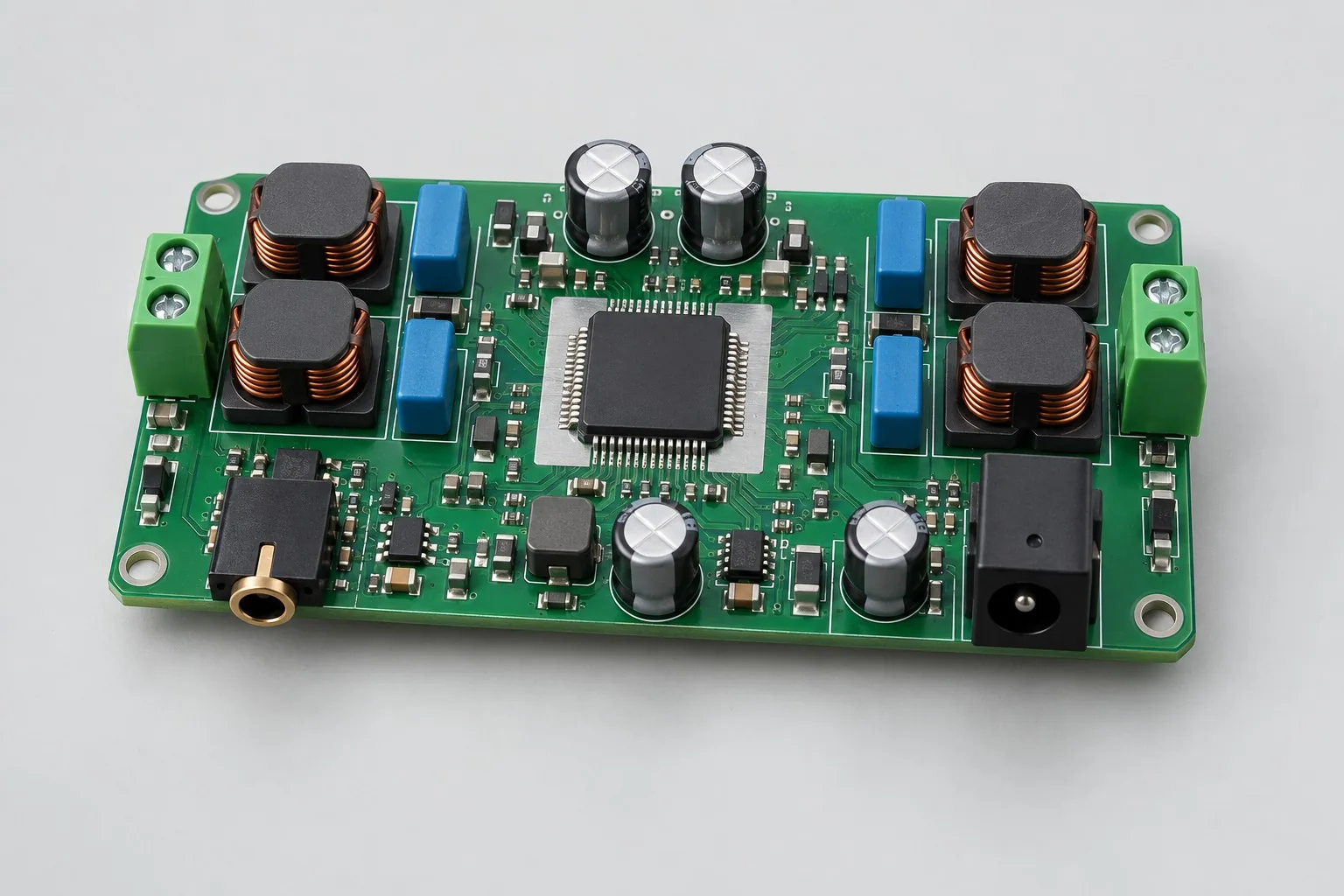
Stereo Class D audio amplifier board design
Return to power amplifier PCB design selection · Select solution by device function · Discuss your design requirements
Documentation Basis and Boundaries
Chinese-language documentation | ADL5602 RF gain block: matching, bias, and linearity tests: ADL5602 supports selection/layout methods for that gain device only; 900MHz is a requirement example. Higher-power PA designs cannot inherit these front-end specifications.