Engineering reference design · prototype validation pending
USB PCB design: USB ports and application endpoints
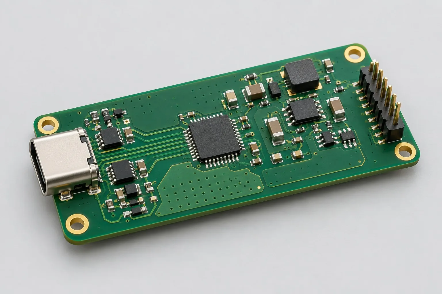
High-speed USB interface boards redesign USB 2.0 High-Speed channels for customer-selected PHY/MCU devices, connecting ports, ESD, and application endpoints. Define device roles/power methods first, then deliver differential layouts, enumeration recovery, and sustained-data tests.
Custom development reference design. The parameters below are requirement configurations and design targets; validate product performance through agreed prototype tests.
| Functional Partition | Design and verification scope |
|---|---|
| USB port and ESD | Select USB-C device-side or Micro-B first; arrange low-capacitance ESD and shield grounding by port. |
| Differential Transmission and Transitions | Target D+/D− at 90Ω; calculate widths/spacing from actual stackups and control stubs, layer changes, and pad transitions. |
| USB Interface controller | Check specified PHY/MCU, clocks, resets, and endpoint capabilities; nominal USB rates are not application throughput. |
| Application/extension interface | Controllers define application frames, endpoint traffic, and buffers; debug interfaces must not add long high-speed stubs. |
| USB Power Management | Confirm bus/self power; design VBUS detection, input protection, and power-off reverse-current blocking. Agree PD separately. |
| Protocol/throughput test | Use specified hosts/cables for enumeration, sustained transfer, sleep/wake, and recovery; separate waveform prescans from formal certification. |
How much does high-speed USB PCB design cost, and how is it quoted?
Do not estimate USB development by differential-pair counts alone. Endpoint functions, PHY, connector protection, and firmware jointly determine work. Type-C power negotiation adds power/software scope. Separate stackup/routing, enumeration/drivers, prototype-link verification, and PD development.
Quotation terms depend on the approved files, quantity, material supply, tests and delivery requirements.
Prepare a structured RFQ or use the short inquiry form.
| Quotation Items | What services are included | What to Check When Comparing Quotes |
|---|---|---|
| Circuit and PCB Design | USB differential constraints, port protection, and power | Reusable portions of existing designs and circuit/mechanical changes |
| Software and Validation | Device enumeration and link test | Define schematics, differential layout, device firmware, host drivers, and link verification separately |
| Prototype Preparation | Bare PCB, BOM procurement, assembly, and agreed prototype quantity | Whether material/component revisions, prototype quantities, and test targets match |
| Subsequent Revision | Record new requirements separately from post-test corrections | How agreed changes, source files, and validation results are delivered |
How does high-speed USB board design differ from Type-C PD design?
USB data channels handle transfer/enumeration; Type-C connectivity and PD negotiation are separate requirements. USB data alone does not establish high-power delivery or full PD functions.
How are trace widths determined for USB differential 90Ω targets?
Calculate using actual fabricator materials, dielectric thickness, copper weight, and spacing, then implement reference planes/transitions. 90Ω is not a fixed width; align stackups before comparing manufacturing options.
Do USB interface design fees include enumeration and drivers?
Define schematics, differential layout, firmware, host drivers, and link verification separately. Impedance fabrication files alone do not establish stable recognition by target hosts.
Reference configuration for USB ports and application endpoints
| Configuration Field | Reference Configurations/Selections | Basis and Status |
|---|---|---|
| Finished Product Function | USB 2.0 High-Speed interface channel | Design Objective |
| Rate Specification | Protocol 480Mb/s target; complete-system acceptance requires testing | Design Objective |
| Connector Options | Choose USB-C device-side or Micro-B | Design Objective |
| Differential Target | D+/D− 90Ω target; no manufacturing-tolerance claim | Design Objective |
| Main Controller Interface | Customer-specified USB PHY/MCU | Design Objective |
| Power Target | VBUS 5V detection; select self/bus power first | Design Objective |
| Protection Configuration | Low-capacitance ESD devices + input power protection | Design Objective |
| Stackup Candidate | 4 layer; signal layer adjacent to ground plane | Design Objective |
| Routing Structure | Few vias, short stubs, continuous reference ground | Design Objective |
| Type-C boundary | CC resistors/controller; no USB PD commitment | Design Objective |
| Firmware Scope | Enumeration, data endpoints, error/reconnection logs | Design Objective |
| Validation outputs | USB waveforms and sustained-data transfer records | Design Objective |
USB device power supply and PD boundary
This page addresses the USB channel for a selected controller; storage mainboards or ADC systems also require data-buffer design.
Basic USB-C devices and PD power negotiation have different scopes; freeze required power roles first.
Protocol requirements define stackup impedance targets; materials/copper weight determine actual widths/spacing.
Design budget and trade-off examples
Check design targets with engineering calculations
For a 480Mbit/s signal timing example, UI is approximately 2.083ns. Eye diagrams, jitter, and return paths still follow device guidance and standard conditions.
Conditions and Scope of Application:This is a rate conversion, not a universal width/length tolerance; nominal rates are not sustained application throughput.
Replace examples with selected components and record margins; calculations support design choices, while prototype records support acceptance.
Power and layout for USB ports and application endpoints
- Place low-parasitic protection near connectors; avoid lengthening D+/D− stubs for probes.
- Keep differential pairs adjacent to continuous ground without crossing splits; review returns at layer changes.
- Check connector, resistor, and ESD pad discontinuities with the complete path.
USB interface board R&D input
- USB roles, connectors, controller models, and data modes
- Fabricator stackups, copper weight, dielectric parameters, and allowable impedance ranges
- VBUS current, shield grounding, cables, and test endpoints
If circuit files exist, provide editable schematics, PCB, BOM, and current issues, and agree on review or revision scope. If only functions are defined, freeze this page's inputs before selection and circuit development. Agree separately on control-software and external-application responsibilities, interfaces, and acceptance.
USB interface board phase delivery
| Stage | Engineering Work for This Proposal | Reviewable Deliverables |
|---|---|---|
| Requirements and Design Freeze | Freeze USB roles, controllers, connectors, endpoint traffic, and power methods | Functional/interface requirements, mechanical revision, acceptance conditions, and open items |
| Schematic and Component Selection | Design PHY/MCU connections, ESD, VBUS management, and basic USB-C CC circuits | Editable schematics, controlled BOM, footprint checks, and design calculations for these circuits |
| Layout and Routing | Route differential channels on approved stackups; review connector/protection pads and returns | PCB source files, actual stackup/hole/net constraints, DRC, and assembly-dimension checks |
| Simulation/Calculation | Calculate impedance/port parasitics, buffering, and net application throughput | Design calculations/models, input conditions, margins, and items awaiting measurement |
| Prototype and Software | Build interface prototypes; integrate enumeration, endpoints, reconnection, and sleep/wake | Manufacturing package, USB prototypes, agreed endpoint firmware, data formats, host-test configurations, and recovery instructions |
| Testing and Version Closure | Regress protocol behavior on specified hosts/cables; measure waveforms and compare impedance records with actual errors | Procedures, wiring, raw results, and decisions for the prototype revision; include issue/change and limitation lists |
USB enumeration and differential waveform verification
- Enumeration, powered/unpowered insertion, sleep/wake, and endpoint faults
- Error rates/dropouts during prolonged full-data transfer
- Differential-waveform/eye-diagram plan under specified test conditions
- Impedance test strip measurement and manufacturing deviation comparison
Regress protocol behavior on specified hosts/cables; measure waveforms and compare impedance records with actual errors. Reports specify equipment, conditions, revisions, and criteria, recording passed and uncovered items.
USB enumeration and differential-waveform verification worksheet
The table converts USB ports/application endpoints into executable checks. Freeze samples, equipment, environments, and allowable deviations before execution; link results to this revision's raw records.
| Verification Object | Pre-Production Freeze | How to Test Prototypes in Practice | Delivery and Acceptance Records |
|---|---|---|---|
| Channel Constraints | Controller/PHY, stackup, connector, ESD devices, and impedance targets | Check differential reference planes, stubs, and protection-device parasitics | Deliver pair constraints, manufacturing stackups, and impedance-coupon records; passing impedance does not establish USB system acceptance |
| Protocol Usage | Hosts, cables, endpoint traffic, and power methods | Regress powered/unpowered insertion, sustained transfer, and sleep/wake | Retain error/dropout/recovery logs; record nominal protocol rates separately from net throughput |
| Waveform Test | Applicable USB test specifications, test points, fixtures, and instrument configurations | Measure differential eyes/electrical specifications under approved test plans | Deliver raw waveforms and criteria; prescan results are not USB certification |
Manufacturing and assembly coordination for this design
- Approve stackups/impedance calculations before trace dimensions; fabricator material changes require review.
- Coupons match product layers/structures; record measurement references/reports by lot.
Link design revisions to schematics, BOM, PCB, fabrication, and software documentation. When fabricators adjust stackup, materials, or holes, or Assembly parties propose substitutions, recheck critical electrical and test conditions together.
Common questions on purchasing and customization
How much does high-speed USB PCB design cost, and how is it quoted?
A project-specific quotation requires review of the available files, quantity, materials, requested tests, delivery destination, taxes, shipping, and trade terms. Any formula on this page organizes cost inputs; it is not a quoted rate.View cost items, calculation conditions, and sources.
Must USB boards be retested after ESD-device changes?
Protection devices are part of the complete channel. Recheck parasitics/layout and regress enumeration/links after substitution, beyond nominal protection ratings.
How is USB-device power-loss recovery accepted?
Test power loss, reconnection, and undervoltage on specified hosts; retain enumeration, firmware-state, and data-recovery records, defining whether interruptions are allowed.
How should USB development budgets be divided by deliverables?
Separate differential layout for existing PHY circuits, enumeration/endpoint software, specified-host sustained transfer, and waveform tests. USB 2.0 HS 480Mb/s is a protocol target; quotations specify actual data tasks/connectors. Itemize Type-C power negotiation and host applications separately from base data-channel costs.
Is a 90Ω target sufficient to start USB routing?
Also provide fabricator stackups, controller PHY, connectors, ESD, and power architecture, defining reference planes/protection locations. Layout delivers D+/D− constraints/manufacturing files; responsible parties separately supply enumeration software/drivers. One impedance value cannot replace complete inputs.
What device work remains when customers provide USB drivers?
Confirm descriptors, endpoints, transfer modes, error returns, and reconnection rules, then implement onboard buffers/logs. Existing drivers reduce host development, but enumeration/sustained transfer still need integration on specified operating systems. One recognition event is not continuous-data acceptance.
How should USB sources and verification packages be delivered?
Retain actual stackups, differential structures, connector/low-capacitance ESD models, VBUS detection, and CC configuration. Software includes descriptors, endpoint protocols, and build environments. Tests identify hosts, cables, reconnection, and sustained-data conditions for later same-channel regression after protection changes.
What work is added when Micro-B changes to USB-C?
Redesign socket pads, CC recognition, and VBUS/ESD; check reversible data connections and fastening. USB protocol software may be reusable, but verify both orientations and specified cables. PD adds negotiation/power design and is not included as a minor connector change.
Can USB2.0 boards directly upgrade to USB3 high-speed transfer?
New channels, PHY, connector pins, and protocols require separate design; existing D+/D− and software do not automatically upgrade. Confirm reusable power/mechanics individually. Quote new SI and host-link tests separately; replacing sockets is not a USB-generation upgrade.
How should quotation documentation be prepared for high-speed USB PCB design?
Initially describe functions, applications, and files. Engineering quotations further confirm USB roles/connectors/controllers/data modes, fabricator stackups/copper/dielectrics/impedance ranges, VBUS current, shield grounding, cables, and endpoints. Provide editable schematics, PCB files, and BOMs for existing designs, or revisions/reproduction records for faulty prototypes. List gaps as review tasks to prevent differing assumptions.
How should high-speed USB PCB prototype verification costs be compared by operating condition?
Fix prototype quantities, revisions, equipment, and criteria sources. Separately review channels: freeze controller/PHY, stackup, connectors, ESD, and impedance; check reference planes/stubs/parasitics. Protocol use: freeze hosts, cables, traffic, and power; regress powered/unpowered insertion, sustained transfer, and sleep/wake. Waveforms: freeze USB specifications, points, fixtures, and instruments; measure eyes/electrical specifications under approved plans. Specify raw-data and issue-closure deliverables; one successful power-up is not complete verification.
Compare related designs and plan the next step
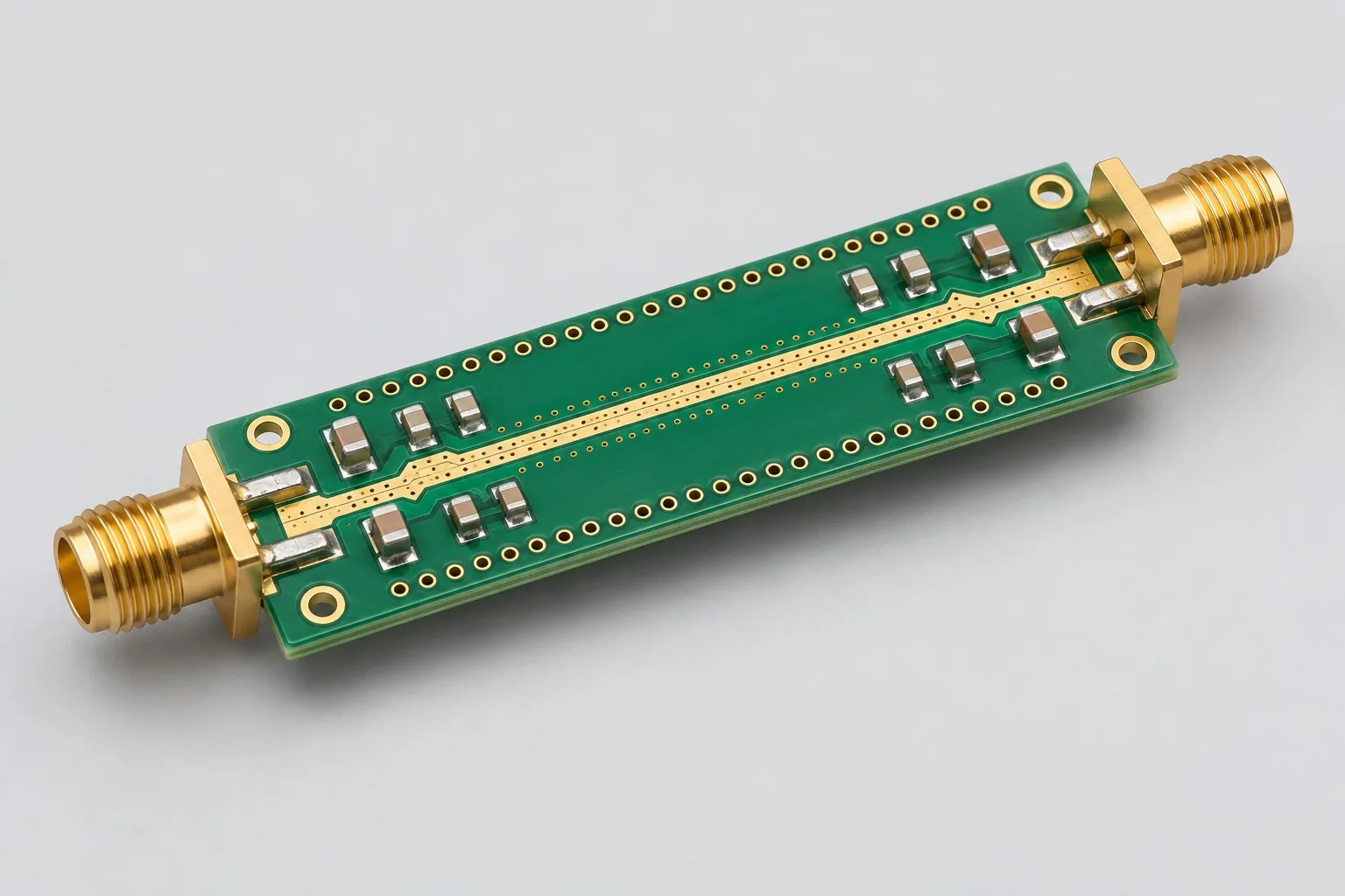
50Ω RF transmission interface board design
Return to impedance-control PCB design selection · Select solution by device function · Discuss your design requirements
Documentation Basis and Boundaries
Chinese-language documentation | USB/high-speed layout: SLLA414 signal-integrity checklist: SLLA414A supports high-speed channel layout; confirm USB electrical criteria, roles, and PHY conditions using actual devices and approved specifications.