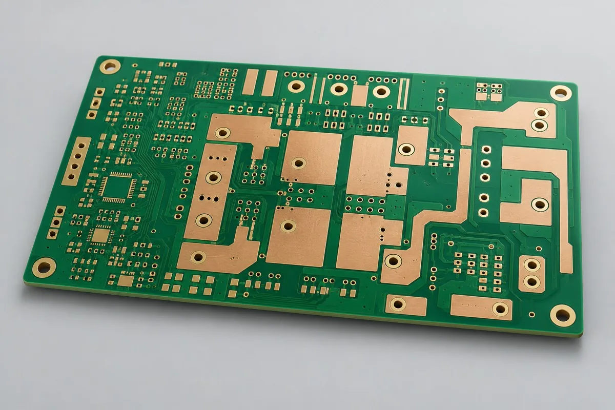
Engineering Reference Configuration
4OZ heavy-copper PCB: four-layer four-ounce OBC fabrication review
Four-layer four-ounce OBC fabrication requires current-drawing review. Bare boards need layer-by-layer copper weights, insulation domains, and large-terminal hole drawings. TG150 4/4OZ is an inherited label with unverified KFPCBA provenance; this page uses an illustrative four-layer heavy-copper configuration. Etching and soldering thermal mass constrain fine-trace space. Deliver microsections, electrical tests, and hole dimensions; bare boards do not guarantee complete-system charging efficiency.
For 4OZ heavy-copper PCBs, first define bare-board prototyping or production scope. Please provide Gerber data, drill files, board outline, and layer stackup, materials/processes, quantity, and fabrication acceptance requirements. The historical four-layer 4/4OZ combination prioritizes heavy-copper etching/resin filling and soldering heat; it is not a renamed six-layer board
Why choose this four-ounce OBC structure
Compare the historical TG150 four-ounce OBC structure when charger power paths are substantial and four layers can accommodate control nets. TG150 4/4OZ prioritizes heavy-copper etching, resin filling, isolation, and soldering heat, avoiding unconditional cost increases through added layers.
What are the key quotation considerations for 4OZ heavy-copper PCBs?
Four-layer 4OZ OBC prices depend on heavy-copper material/finished definitions, etch spacing, lamination resin filling, power-lead holes, and high-thermal-mass pads. List lead-free HASL separately from actual assembly verification. Historical TG150 and 4/4OZ are starting records; current materials, thickness, and insulation still require fabrication drawings rather than ordinary four-layer unit prices.
Quotation terms depend on the approved files, quantity, material supply, tests and delivery requirements.
Prepare a structured RFQ or use the short inquiry form.
Enter the following items in one itemized quotation: specify cost units and tax/shipping basis, with separate columns for first orders and same-revision repeat orders. The table is a procurement breakdown method, not a ready-made price list; reference specifications require approval against current fabrication drawings.
| Quotation items and pricing boundaries | Configuration inputs to confirm | Repeat orders and revision changes |
|---|---|---|
| Materials/fabrication, quoted per batch or accepted board | Historical TG150 grade unlisted; procure from an approved TG150-grade material list as reference; 4-layer through-hole board; historical 4/4OZ does not distinguish base/finished copper; reference inner 140µm, outer base 105µm/finished 140µm | Recurs on repeat orders; material, layer-order, or copper-weight changes require requotation |
| Holes and forming, per approved hole table | Historical through-holes; Ø0.50mm through-hole reference target, with power-pin holes sized to components | Reorders follow the same revision; review operations before 4OZ/high-voltage partition changes |
| Surface finish/packaging, noting areas and batches | Reference lead-free HASL; verify heavy-copper pad temperature profiles separately | Incurred by actual batch; confirm packaging, storage conditions, and surface-finish substitutions separately |
| Engineering/tooling preparation, identifying one-time or per-batch charges | 4OZ/high-voltage partitioning: provide OBC power nets, insulation boundaries, and each layer's 4OZ definition. | Verify file revisions, ownership, and storage condition before reusing old tooling; do not assume reuse is free |
| Structural/special inspections, identifying coupons, hole groups, or samples | Retain copper-weight/clearance approvals and microsection results; specify dielectric-withstand conditions separately for this order. Critical hole-wall copper and pad dimensions support assembly first-article verification. | List initial prototype validation and per-batch sampling separately; quote per-board requirements separately rather than assuming everything is completed once |
| Delivery scope, reports, and accepted quantity | Four-layer 4oz reference-design bare PCB, copper-weight/isolation-domain drawings, microsections/electrical tests, and agreed soldering/thermal verification data. | Retain revision links and batch records on repeat orders; list component assembly, firmware, and complete-unit testing separately |
How should four-layer 4OZ OBC and six-layer 3OZ boards be selected?
Four-layer 4OZ prioritizes heavier power paths; six-layer 3OZ provides more control-routing resources. Check whether four layers accommodate control nets, then high-current path widths and thermal conditions. Thicker 4OZ does not make all performance interchangeable; compare layer count, copper weight, and copper allocation together.
| Comparison Dimension | 4 oz heavy-copper PCB fabrication | 3 oz heavy-copper PCB fabrication |
|---|---|---|
| Material and Grade | Historical TG150 grade unspecified; reference procurement from an approved material list meeting TG150 grade | Historical TG170 grade unlisted; S1000-2M is a reference material candidate |
| Layer Count and Structure | 4 Layer Through-Hole Board | 6 Layer Through-Hole Board |
| Hole Structure and Dimensions | Historical through-holes; Ø0.50mm through-hole reference target, with power-pin holes sized to components | Historical through holes; Ø0.40mm through-hole reference target, with power layer-transition via arrays |
| Application | OBC charger modules; bare high-current power-conversion boards | Automotive portable power supplies; medium/high-current DC power bare boards |
Can 4OZ spacing and board thickness follow ordinary PCB rules?
Thicker-copper etching needs different geometric allowances; this page's 0.40mm reference spacing is not a system safety clearance. Evaluate total thickness, adjacent dielectrics, and resin filling together; terminal holes also need component drawings. Define high-voltage isolation before power layout rather than compressing spacing with ordinary fine-trace rules.
| Decision Sequence | Required project inputs | Agreed records and deliverables |
|---|---|---|
| 1. Define application and scope | Provide OBC power nets, insulation boundaries, and each layer's 4OZ definition. | Retain copper-weight/clearance approvals and microsection results; specify dielectric-withstand conditions separately for this order. |
| 2. Confirm structural requirements | List large-terminal holes, power pads, and solder-mask openings, distinguishing bare-board manufacturability from assembly solderability. | Critical hole-wall copper and pad dimensions support assembly first-article verification. |
| 3. Align nets with fabrication targets | No impedance control for power nets; verify drive loops and insulation regions according to circuit design | Provide target nets, layer pairs, and verification scope; review with historical through holes, Ø0.50mm through-hole reference targets, and power-lead holes sized to components |
| 4. Confirm quotation and release revision | Historical TG150 grade unlisted; reference procurement from an approved TG150-grade material list; 2.40mm reference target confirmed against design targets; reference lead-free HASL; verify heavy-copper pad profiles separately | Request quotations using material/pattern/inspection lists at the same revision; list unapproved substitutions as separate alternatives rather than including them in the baseline quotation |
Four-Ounce OBC Board Manufacturing Specifications
| Specification Items | Reference configuration or target |
|---|---|
| Illustrative structure to define | Illustrative OBC bare PCB: four-layer through-hole construction; approve the actual material and copper definition; no charging-efficiency result is claimed |
| Material and Grade | Historical TG150 grade unspecified; reference procurement from an approved material list meeting TG150 grade |
| Layer Count and Structure | 4 Layer Through-Hole Board |
| Total Board Thickness | 2.40mm reference target; confirm against design targets |
| Dielectric thickness and interlayer relationship | 0.25mm reference target adjacent to heavy copper; design insulation distances separately |
| Base Copper and Finished Copper | Historical 4/4OZ does not distinguish base/finished copper; reference inner 140µm, outer base 105µm/finished 140µm |
| Hole Structure and Dimensions | Historical through-holes; Ø0.50mm through-hole reference target, with power-pin holes sized to components |
| Trace Width and Spacing | 0.40/0.40mm reference design; size high-current paths separately |
| Impedance Target and Measurement Methods | No impedance control for power nets; verify drive loops and insulation regions according to circuit design |
| Surface Finish | Reference lead-free HASL; verify heavy-copper pad temperature profiles separately |
| Application | OBC charger modules; bare high-current power-conversion boards |
| Deliverables | Four-layer 4oz reference-design bare PCB, copper-weight/isolation-domain drawings, microsections/electrical tests, and agreed soldering/thermal verification data. |
Tradeoffs between four-ounce routing space and soldering thermal mass
Four-ounce copper reduces fine-routing space, while large-pad thermal mass affects soldering windows. Historical TG150 markings do not establish all high-temperature applications, and historical configurations do not quantify OBC power/voltage. Define internal insulation and cooling from actual topology and components.
Heavy-copper resin filling, power-lead holes, and insulation domains: manufacturing checks
Reference 0.40mm spacing describes manufacturable geometry only; voltage/environment determine safety distances. Adjacent-layer 0.25mm is a resin-fill starting point. Fabrication/assembly drawings must agree on inner/outer copper definitions, depanelization, and high-thermal-mass pads.
Heavy-copper microsections and power-region electrical tests: acceptance items
Microsections inspect heavy-copper edges, hole-wall copper, and resin filling; bare-board electrical/insulation tests follow project requirements. Assembled prototypes then verify power loops, temperature rise, and soldering quality; historical bare-board configurations cannot promise complete-system charging efficiency.
Four-ounce OBC board delivery scope
Applications: OBC charging modules; high-current power-conversion bare boards.
Four-layer 4oz reference-design bare PCB, copper-weight/isolation-domain drawings, microsections/electrical tests, and agreed soldering/thermal verification data.
Layer-specific 4OZ definitions and large-terminal openings: quotation inputs
Submit layer-specific 4OZ definitions and large-terminal openings, converting tabled design targets into inspectable drawings. The following inputs separately define artwork, material, or structural inspection scope; freeze quotation revisions with approved drawings.
| Project inputs required for review | Engineering decisions | Records/delivery as agreed in the order |
|---|---|---|
| 4OZ and High Voltage Partitioning | Provide OBC power nets, insulation boundaries, and each layer's 4OZ definition. | Retain copper-weight/clearance approvals and microsection results; specify dielectric-withstand conditions separately for this order. |
| Soldering Thermal Mass | List large-terminal holes, power pads, and solder-mask openings, distinguishing bare-board manufacturability from assembly solderability. | Critical hole-wall copper and pad dimensions support assembly first-article verification. |
4OZ heavy-copper PCB fabrication: pricing, selection, and procurement FAQ
What are the key quotation considerations for 4OZ heavy-copper PCBs?
A project-specific quotation requires review of the available files, quantity, materials, requested tests, delivery destination, taxes, shipping, and trade terms. This is not a complete finished-product quotation. Base fabrication/sample pricing, special processes, and inspections must not be billed twice. No current unit prices are published here; request an itemized quotation for the approved scope.Review quotation inputs and scope.
How should four-layer 4OZ OBC and six-layer 3OZ boards be selected?
Four-layer 4OZ prioritizes heavy power paths, while six-layer 3OZ adds control-routing resources; neither is a simple upgrade. Confirm four-layer control routability, then copper paths/holes and temperature rise; select layer count and copper weight together. Review the comparison
Can 4OZ spacing and board thickness follow ordinary PCB rules?
Ordinary fine-trace rules cannot be applied directly; heavy copper needs appropriate etching/resin-fill space. 0.40mm is this page's fabrication reference, not a safety-isolation rule. Evaluate total thickness, adjacent dielectric, and power-lead holes against actual voltage, components, and soldering. Review the comparison
Does 4OZ on an OBC board guarantee charging efficiency?
No. Topology, components, switching, magnetic components, and cooling jointly determine efficiency. Bare-board inspections check power-region copper weight, hole-wall copper, and insulation; measure final efficiency in the assembled system under specified loads.
Why do 4OZ pads need separate soldering verification?
More copper and thicker boards increase thermal mass and may change through-hole solder penetration and reflow windows. Design copper paths and thermal connections with assembly processes; ordinary-board profiles alone are insufficient.
Can a 4OZ quote assume TG170 material?
The inherited TG150 label is not a confirmed material grade for a current order; do not make silent substitutions. If the current order changes material grade, identify its model and recheck stackup, thermal processes, and costs rather than retaining only the OBC title.
Which bottlenecks need checking before changing a 4OZ OBC board to 3OZ to save cost?
Check power-path lengths, neck-downs, vias, and terminals, then assess reduced copper against allowed voltage drop, temperature rise, and insulation. Thinner copper may reduce fabrication work but requires geometric updates and verification; old current-capacity conclusions cannot remain. Confirm soldering thermal mass using actual assembly.
How are per-board and per-panel 4OZ heavy-copper quotations converted?
Review panelization for 4OZ etching/resin filling and large-pad thermal mass, retaining power-lead holes and isolation boundaries; do not estimate material using ordinary four-layer fine-trace rules. State deliverable boards per panel, purchased panels, and board/panel delivery condition. Divide actual panel fabrication charges by corresponding accepted board count; list setup, specialized inspections, and packaging separately, without promising yield from theoretical utilization.
How should first-order one-time charges and reorder costs be separated for 4OZ heavy-copper fabrication?
First confirm 4OZ/high-voltage partitioning and soldering thermal-mass documentation, stating whether engineering, tooling, or test setup is charged once. Retain copper-weight/clearance approvals and microsections; specify withstand conditions separately. Verify files and ownership before tool reuse; current materials, fabrication, and approved inspections still incur costs. List renewed preparation after changes separately rather than using the old total alone.
Can I obtain a 4OZ heavy-copper budget before 4OZ/high-voltage partition documentation is complete?
Describe application, outline, quantity, and drawings for a budget identifying gaps. Formal review needs OBC power nets, insulation boundaries, and each layer's 4OZ definition. Deliver copper-weight/clearance approvals and microsections, with withstand conditions separately specified. Confirm fabrication/inspection quotes after conditions freeze. Initial inquiries need not include every file, but estimates do not cover undefined structures by default.
What must be reconfirmed when materials, hole tables, or installation conditions change on a 4OZ heavy-copper reorder?
List large-terminal holes, power pads, and mask openings, distinguishing manufacturability from assembly solderability. Critical hole-wall copper/pad records support assembly first articles. Map changes to old material/hole-table/mechanical files to identify drawing, process, or measurement updates; unchanged product names and layer counts do not establish identical reorder conditions.
If two 4OZ heavy-copper quotes use the same material, which configurations still need comparison?
Check historical TG150 against current grade, 4OZ base/finished definitions, and power holes; compare insulation/soldering conditions separately. 4-layer 4OZ is not a direct upgrade from 6-layer 3OZ.
Which reports should link to board identifiers before 4OZ heavy-copper prototypes enter production?
Retain copper-weight/clearance approvals and microsections; specify withstand conditions separately. Critical hole-wall copper/pad dimensions support assembly first articles. Link material lots, approved files, and results to current samples; production uses the revision with issues closed. Old coupon/artwork reports support comparison but cannot replace current inputs; define uncovered complete-system objects separately.
When small-batch 4OZ heavy-copper unit prices fall, how can I tell whether total procurement costs decreased?
Compare lower-copper alternatives against identical OBC targets, including recalculation of neck-downs/via arrays and soldering verification. Material savings alone do not establish retained functions and lower totals. Add setup, fabrication, agreed inspections, packaging, and freight, then divide by accepted delivery quantity for equal-scope total and unit comparisons. Use current quoted rates; assume no fixed discount.
Four-ounce OBC boards compared with related board types
Current distinction: historical four-layer 4/4OZ prioritizes heavy-copper etching/resin filling and soldering heat; it is not a renamed six-layer board
- Six-layer TG170 three-ounce portable power board — Historical six-layer TG170 3/3OZ combination; current capacity depends on copper cross-sections, via arrays, and cooling boundaries
- Six-layer partial buried copper block power control board — Local copper blocks concentrate current/heat without sacrificing signal density through whole-board heavy copper; embedded-copper processes require separate review
Heavy copper board complete product catalog · All PCB Products
Design and assembly responsibilities for four-ounce OBC boards
Related Functional Directions:Energy Storage Power Interface Board · Isolated power and control interface board design. These pages compare design or assembly responsibilities in the same application area. Materials, layer counts, components, and interface configurations differ; they do not share one physical model and are not extended delivery records for this engineering reference configuration.
Bare PCB validation on this page covers agreed materials, patterns, continuity/insulation, stackup, and test coupons. Design work separately covers circuits, models, and drawings; PCB assembly separately covers BOM components, soldering, firmware, and post-assembly functional tests. Before moving to related services, remap scope using final drawings/BOM; bare PCB reports cannot replace complete-unit acceptance.
Material and design basis for four-ounce OBC boards
- Engineering reference | PCB thermal estimates: power dissipation, copper area, and junction-temperature checks: Thermal design methods
When citing these resources, record material revisions and design conditions for the historical TG150 4/4OZ copper combination; first articles focus on heavy-copper microsections and power-region electrical tests. Update drawings and inspections after material, copper-weight, or hole changes before release.
Request Quote for This PCB Configuration: cite product ID 247, attach critical circuit/interface information and quantity, and list specifications to retain or adjust.