Engineering Selection Reference
Six-layer PCB prototyping: six-layer impedance-verification sample fabrication review
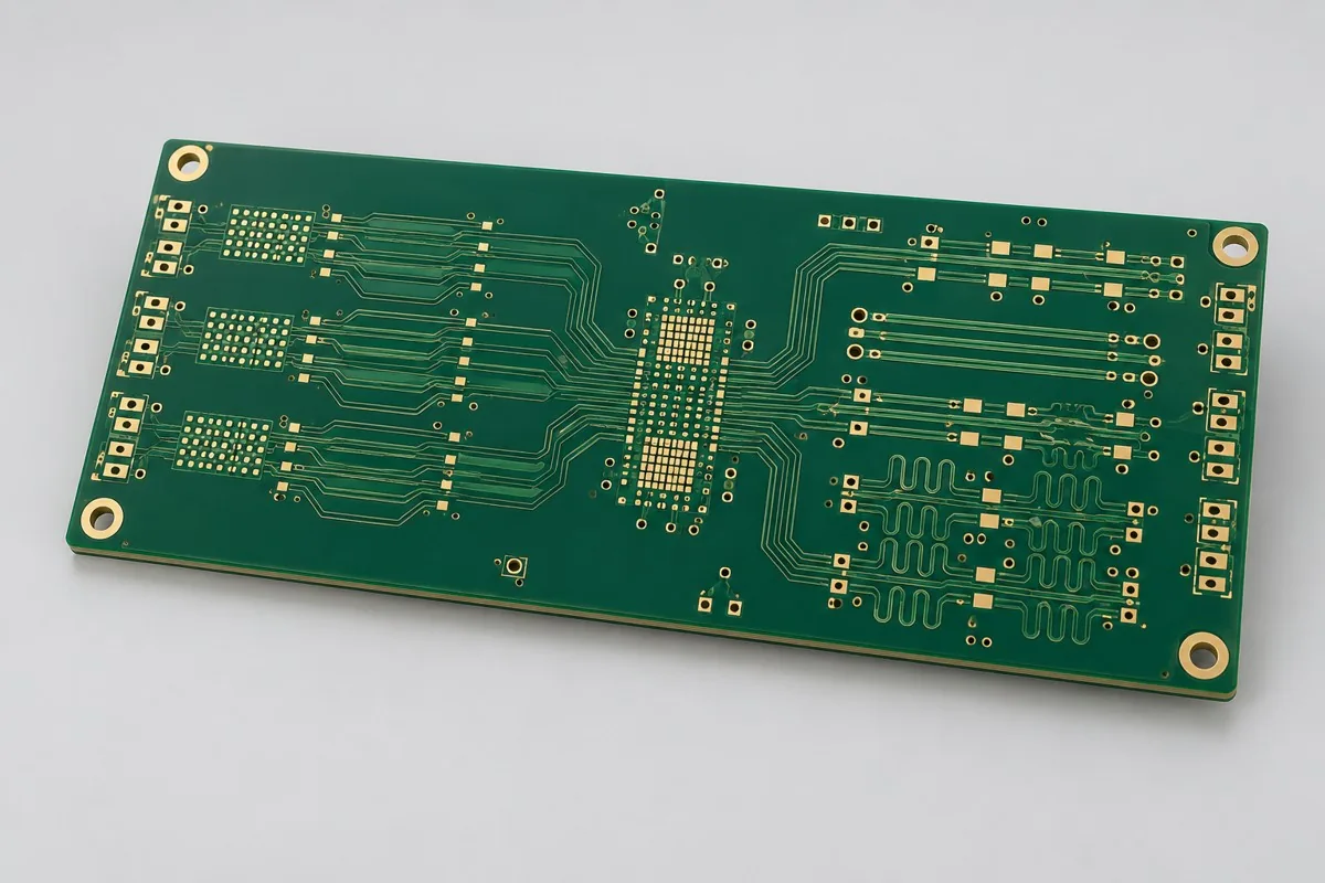
Six-layer impedance-verification sample fabrication requires current-drawing review. Six-layer differential-interface bare-board prototypes require target-net definitions, actual layer pairs, and same-panel coupon drawings. Coupons represent manufacturing geometry and cannot cover the entire component link; deliver raw TDR curves, layer-transition structures, and measured stackup records; 50Ω/100Ω are adjustable reference starting points only.
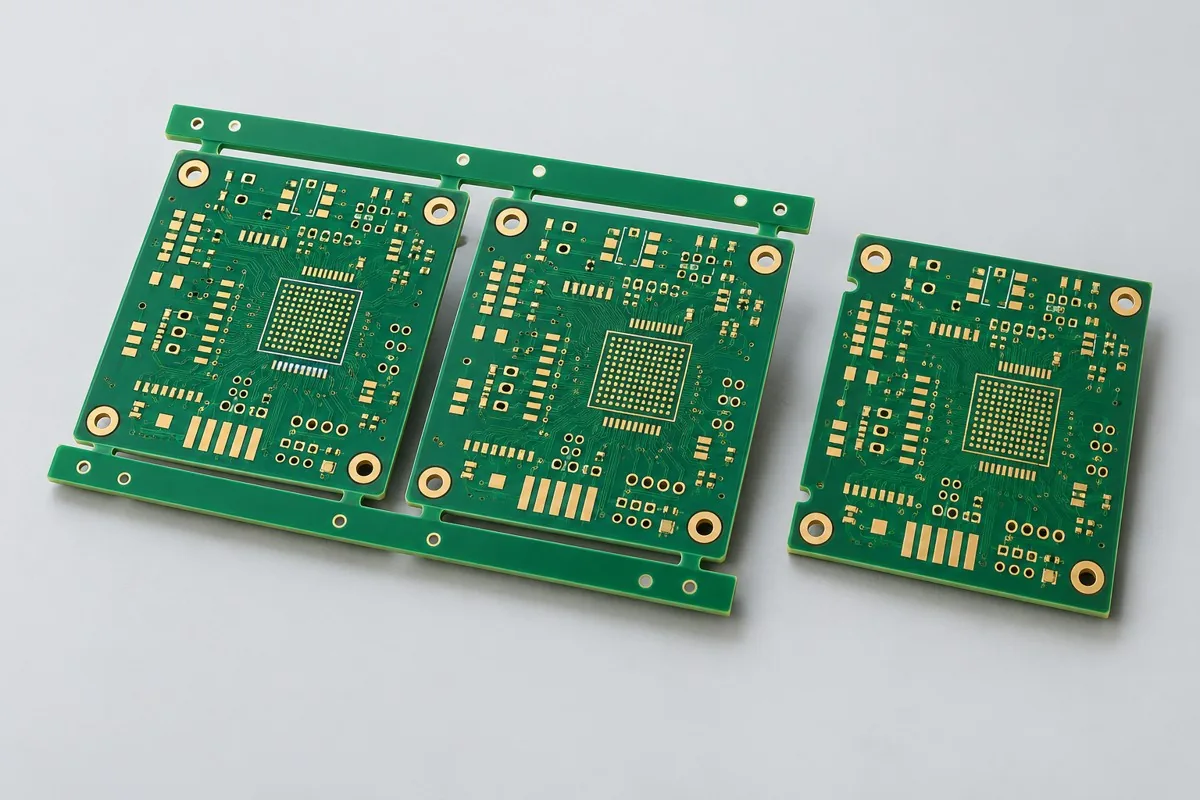
Six-layer PCB prototyping first requires a defined bare-board prototype or production scope. Provide Gerber, drills, stackup, materials/processes, quantity, and fabrication acceptance requirements. Six-layer samples include impedance coupons and link-test structures as deliverables, unlike four-layer functional samples
Why choose this structure for six-layer impedance prototype
Six-layer impedance samples suit high-speed interface prototypes requiring fabrication-stackup and actual transmission-geometry verification. They include 50Ω/100Ω target coupons, actual layer pairs, and critical layer-transition structures as same-panel deliverables, making material/geometric deviations easier to identify than with four-layer samples checking only functional continuity.
Why does six-layer impedance PCB prototyping cost more than ordinary functional samples?
Six-layer fabrication, target-net stackup control, same-panel impedance coupons, TDR records, and necessary layer-transition structures incur different costs. Quotations must state coupon layer pairs and sample quantities; S-parameter testing is separate. Four-layer pricing covering only netlist electrical tests is not directly comparable. Samples and production must use identical materials and geometry for test results to guide subsequent procurement.
Quotation terms depend on the approved files, quantity, material supply, tests and delivery requirements.
Prepare a structured RFQ or use the short inquiry form.
Enter the following items in one itemized quotation: specify cost units and tax/shipping basis, with separate columns for first orders and same-revision repeat orders. The table is a procurement breakdown method, not a ready-made price list; reference specifications require approval against current fabrication drawings.
| Quotation items and pricing boundaries | Configuration inputs to confirm | Repeat orders and revision changes |
|---|---|---|
| Materials/fabrication, quoted per batch or accepted board | Isola 370HR FR4 reference candidate; measured stackup parameters fed back; 6 layers; inner copper 18µm; outer base 18µm/finished target 35µm | Recurs on repeat orders; material, layer-order, or copper-weight changes require requotation |
| Holes and forming, per approved hole table | Ø0.25mm through holes; return vias beside critical layer transitions | Reorders follow the same revision; review processes before differential-verification coupon changes |
| Surface finish/packaging, noting areas and batches | ENIG; coupons share the main board's panel and surface finish | Incurred by actual batch; confirm packaging, storage conditions, and surface-finish substitutions separately |
| Engineering/tooling preparation, identifying one-time or per-batch charges | Differential-verification coupons: provide target nets, layer numbers, trace width/spacing, reference layers, and coupon locations. | Verify file revisions, ownership, and storage condition before reusing old tooling; do not assume reuse is free |
| Structural/special inspections, identifying coupons, hole groups, or samples | Feed measurements back into corresponding stackup models; retain raw curves and coupon/board numbers. Record changes and impedance results for each revision; production revision changes require renewed approval. | List initial prototype validation and per-batch sampling separately; quote per-board requirements separately rather than assuming everything is completed once |
| Delivery scope, reports, and accepted quantity | Six-layer bare PCB samples, same-panel impedance/layer-transition coupons, measured stackup records, TDR data, and documentation revisions for production freeze. | Retain revision links and batch records on repeat orders; list component assembly, firmware, and complete-unit testing separately |
How do six-layer impedance samples differ from four-layer functional boards?
Four-layer functional boards prioritize component and circuit debugging; six-layer impedance samples focus on fabrication stackup and actual transmission geometry. Interface issues require identical layer pairs and transition structures. Low-speed MCU logic does not require coupons for every trace. Select according to issues requiring closure; layer count alone does not indicate sample quality.
| Comparison Dimension | Six-layer impedance PCB prototyping | Four-Layer PCB Prototype |
|---|---|---|
| Material and Grade | Isola 370HR FR4 reference candidate; measured stackup parameters fed back | Shengyi S1000-2M FR4 reference grade, sample material lots retained |
| Layer Count and Structure | 6 Layer | 4 Layer |
| Hole Structure and Dimensions | Ø0.25mm through holes; return vias beside critical layer transitions | Ø0.30mm through holes; filling or blind vias not included by default |
| Application | High-speed interface prototype; acquisition link prototype | MCU functional prototypes; small-batch control-board verification |
How should 50Ω, 100Ω, and tolerances be selected for impedance samples?
Determine targets and tolerances from interface and chip requirements; 50Ω/100Ω are only this page's starting points. List actual layer pairs, solder mask, and copper weight for each net group; coupons replicate corresponding main-board structures. Adjust the net table for special interfaces requiring different targets instead of applying identical values universally.
| Decision Sequence | Required project inputs | Agreed records and deliverables |
|---|---|---|
| 1. Define application and scope | Provide target nets, layer numbers, trace width/spacing, reference layers, and coupon locations. | Feed measurements back into corresponding stackup models; retain raw curves and coupon/board numbers. |
| 2. Confirm structural requirements | Specify whether this iteration calibrates dielectric thickness or adjusts trace width; changing multiple variables simultaneously can make the causes of deviation harder to identify. | Record changes and impedance results for each revision; production revision changes require renewed approval. |
| 3. Align nets with fabrication targets | 50Ω single-ended/100Ω differential reference targets; layer-specific TDR; special-interface targets agreed separately | Provide target nets, layer pairs, and verification scope; review together with Ø0.25mm through holes and return vias beside critical layer transitions |
| 4. Confirm quotation and release revision | Isola 370HR FR4 reference candidate; measured stackup parameters fed back; 1.60mm reference target; ENIG; coupons share the main board's panel and surface finish | Request quotations using material/pattern/inspection lists at the same revision; list unapproved substitutions as separate alternatives rather than including them in the baseline quotation |
Six-layer impedance prototype manufacturing specifications
| Specification Items | Reference configuration or target |
|---|---|
| Material and Grade | Isola 370HR FR4 reference candidate; measured stackup parameters fed back |
| Layer Count and Structure | 6 Layer |
| Total Board Thickness | 1.60mm reference target |
| Dielectric thickness and interlayer relationship | Target signal-to-ground spacing 0.12mm; coupons replicate actual layer pairs |
| Base Copper and Finished Copper | Inner copper 18µm; outer base 18µm/finished target 35µm |
| Hole Structure and Dimensions | Ø0.25mm through holes; return vias beside critical layer transitions |
| Trace Width and Spacing | 0.10/0.10mm reference design |
| Impedance target and measurement method | 50Ω single-ended/100Ω differential reference targets; layer-specific TDR; special-interface targets agreed separately |
| Surface Finish | ENIG; coupons share the main board's panel and surface finish |
| Application | High-speed interface prototype; acquisition link prototype |
| Deliverables | Six-layer bare PCB samples, same-panel impedance/layer-transition coupons, measured stackup records, TDR data, and documentation revisions for production freeze. |
Tradeoffs between coupon representativeness and complete-link coverage
Same-panel coupons help control manufacturing consistency but do not cover every mismatch in connectors, vias, and the complete link. Six layers add verification resources and sample costs. If the interface specifies other targets, revise the net table instead of imposing 50/100Ω.
Main-board layer-pair coupons and measured stackup feedback: manufacturing checks
Coupon dielectric thickness, copper weight, solder mask, and finish match the main board; measurement connections must support repeatable positioning. Name critical transition structures separately and feed first-article measurements back into the manufacturing stackup instead of retaining only uncorrected initial EDA values.
Layer-specific TDR and optional transition S-parameters: acceptance items
TDR records include layer pairs, targets, measured curves, and instruments/connection methods; use S-parameters to compare link structures when necessary. Verify interface speed/error rate on prototypes, then approve the final material/geometric revision before production to prevent incorrect data attribution.
Six-layer impedance prototype delivery scope
Applications: high-speed interface prototypes; acquisition-link samples.
Six-layer bare PCB samples, same-panel impedance/layer-transition coupons, measured stackup records, TDR data, and documentation revisions for production freeze.
Target nets, coupon locations, and individual revisions: quotation inputs
Submit target nets, coupon locations, and individual revisions to convert tabled design targets into inspectable fabrication drawings. The following inputs determine artwork, material, or structural inspection scope; the quotation revision freezes with approved drawings.
| Project inputs required for review | Engineering decisions | Records/delivery as agreed in the order |
|---|---|---|
| Differential-impedance coupons | Provide target nets, layer numbers, trace width/spacing, reference layers, and coupon locations. | Feed measurements back into corresponding stackup models; retain raw curves and coupon/board numbers. |
| Revision approval and feedback | Specify whether this iteration calibrates dielectric thickness or adjusts trace width; changing multiple variables simultaneously can make the causes of deviation harder to identify. | Record changes and impedance results for each revision; production revision changes require renewed approval. |
Six-layer impedance PCB prototyping: pricing, selection, and procurement FAQs
Why does six-layer impedance PCB prototyping cost more than ordinary functional samples?
A project-specific quotation requires review of the available files, quantity, materials, requested tests, delivery destination, taxes, shipping, and trade terms. Add specified materials, processes, and inspections not yet included to the total cost. Standard board references do not cover every configuration of this product. No current unit prices are published here; request an itemized quotation for the approved scope.Review quotation inputs and scope.
How do six-layer impedance samples differ from four-layer functional boards?
Six-layer impedance samples focus on actual stackup, transmission lines, and specified transitions; four-layer functional boards focus on components and ordinary circuit functions. Connectors and loads still require actual prototype testing. Select according to issues requiring closure; six layers are not inherently better than four. Review the comparison
How should 50Ω, 100Ω, and tolerances be selected for impedance samples?
50Ω/100Ω are reference targets only; actual targets and tolerances depend on interfaces/chips. List actual layer pairs, copper weight, and solder mask for each net group; coupons replicate corresponding main-board structures. Special interfaces must not be assigned common impedance values simply to simplify testing. Review the comparison
Does six-layer impedance prototyping pricing include TDR curves?
Specify layer pairs, targets, samples, measurement connections, and curve delivery instead of merely stating controlled impedance. A pass statement and reviewable data represent different scopes; align these when comparing quotations.
Does a passing impedance coupon guarantee the complete link?
Coupons do not cover all main-board connectors, vias, and loads. Critical transitions can use separate test structures; verify interface speed and error rate on actual component prototypes. Coupons help explain manufacturing consistency.
Can impedance samples change to equally thick materials for production?
Equal thickness does not mean equal Dk, copper foil, or loss. Retain approved materials and measured stackups; recalculate geometry and reverify substitutions. Old coupon reports cannot validate a new lot's structure.
Will changing trace width and dielectric thickness together speed up six-layer impedance prototype convergence?
Simultaneous changes make deviation sources difficult to identify. To calibrate manufacturing models, hold other variables constant and change one parameter, retaining coupon numbers, stackups, and raw curves. If combined changes are necessary, identify each in a new simulation revision and verify the new structure.
How are per-board and per-panel six-layer impedance prototyping quotations converted?
Impedance coupons replicate actual main-board layer pairs and carry same-panel identifiers; record transition structures and revisions separately. Generic coupon area cannot replace actual measurement arrangements. State deliverable finished boards per panel, actual panels purchased, and individual-board/panel delivery format. Calculate fabrication cost per board by dividing actual panel fabrication charges by corresponding accepted finished boards. List setup, special inspections, and packaging separately; theoretical utilization does not guarantee yield.
How are first-order one-time costs separated from six-layer impedance prototyping reorder costs?
First confirm differential-verification coupon and closed-loop revision documentation, stating whether engineering, tooling, or test setup is charged once. Feed measurements back into corresponding stackup models; retain raw curves and coupon/board numbers. Confirm files and ownership before reusing tools. Current-lot materials, fabrication, and approved inspections still incur costs; separately list setup repeated after changes instead of reusing the old order total.
Can I obtain a six-layer impedance prototyping budget before differential-verification coupon documentation is complete?
Provide the application, board outline, quantity, and available drawings for a budget identifying missing inputs. Formal review requires target nets, layer numbers, trace width/spacing, reference layers, and coupon locations. Corresponding delivery includes measured-data feedback into stackup models, raw curves, and coupon/board numbers. Confirm fabrication/inspection pricing after these conditions freeze. Initial inquiries need not include every file, but estimates do not cover undefined structures.
What requires reconfirmation when six-layer impedance prototype reorders change materials, hole tables, or mounting conditions?
Specify whether this iteration calibrates dielectric thickness or adjusts trace width; changing multiple variables simultaneously can make the causes of deviation harder to identify. Record changes and impedance results for each revision; production revision changes require renewed approval. Match each change against prior material/hole-table/mechanical files to determine drawing revisions, process changes, or remeasurement. The same product name and layer count do not establish identical reorder conditions.
What configurations should be compared when two six-layer impedance prototyping quotations use the same material?
Check actual 50Ω/100Ω nets and tolerances, coupon layer pairs/solder mask, and raw TDR delivery. Separate dielectric-thickness or trace-width revisions; old curves do not cover new manufactured structures.
Which reports must link to board numbers before six-layer impedance PCB samples enter production?
Feed measurements back into corresponding stackup models; retain raw curves and coupon/board numbers. Record changes and impedance results for each revision; production revision changes require renewed approval. Link material lots, approved fabrication files, and inspection results to current sample numbers; production uses the revision with issues closed. Old coupon or artwork-revision reports support comparison but cannot replace current manufacturing inputs. Define separate scope for complete-system items not yet covered.
How can lower small-batch six-layer impedance prototype unit prices be checked against total procurement costs?
Shared coupon setup may reduce repeated work, but retain measurements separately for different layer pairs and revisions. A pass statement and raw TDR curves represent different quotation scopes. Add setup, fabrication, agreed inspections, packaging, and shipping, then divide by accepted delivery quantity to compare equal-scope total and per-board costs. Use the current inquiry for amounts and rates; do not assume fixed reductions.
Comparison of six-layer impedance prototype with adjacent board types
Current configuration distinction: six-layer samples include impedance coupons and link-test structures as deliverables, unlike four-layer functional samples
- Four-layer FR4 general functional verification prototype — Four-layer through holes verify functions/assembly; Gerber comparisons and sample revisions support production transition
PCB Sample complete product catalog · All PCB Products
Six-layer impedance prototype material and design basis
- Engineering reference | Isola 370HR material: high Tg and frequency-dependent parameters: Published manufacturer material data
- Engineering reference | General high-speed interface layout: return paths, length, and layer transitions: Design methodology
- Engineering reference | Gerber manufacturing data: layer functions, drilling, and attributes: Manufacturing File Format
When citing these sources, record material revisions and design conditions for six-layer same-panel impedance and transition coupons. First-article checks cover layer-specific TDR curves; transition S-parameters are measured separately under agreement only when needed. Update fabrication drawings and inspections before releasing changes to materials, copper weight, or hole structures.
Request Quote for This PCB Configuration: Reference product ID 249, attach critical circuits/interfaces and quantities, and list specifications to retain or adjust.