Engineering Selection Reference
Double-sided PCB fabrication: double-sided FR4 instrument interface board fabrication review
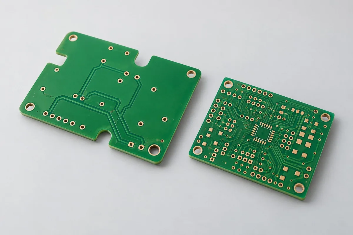
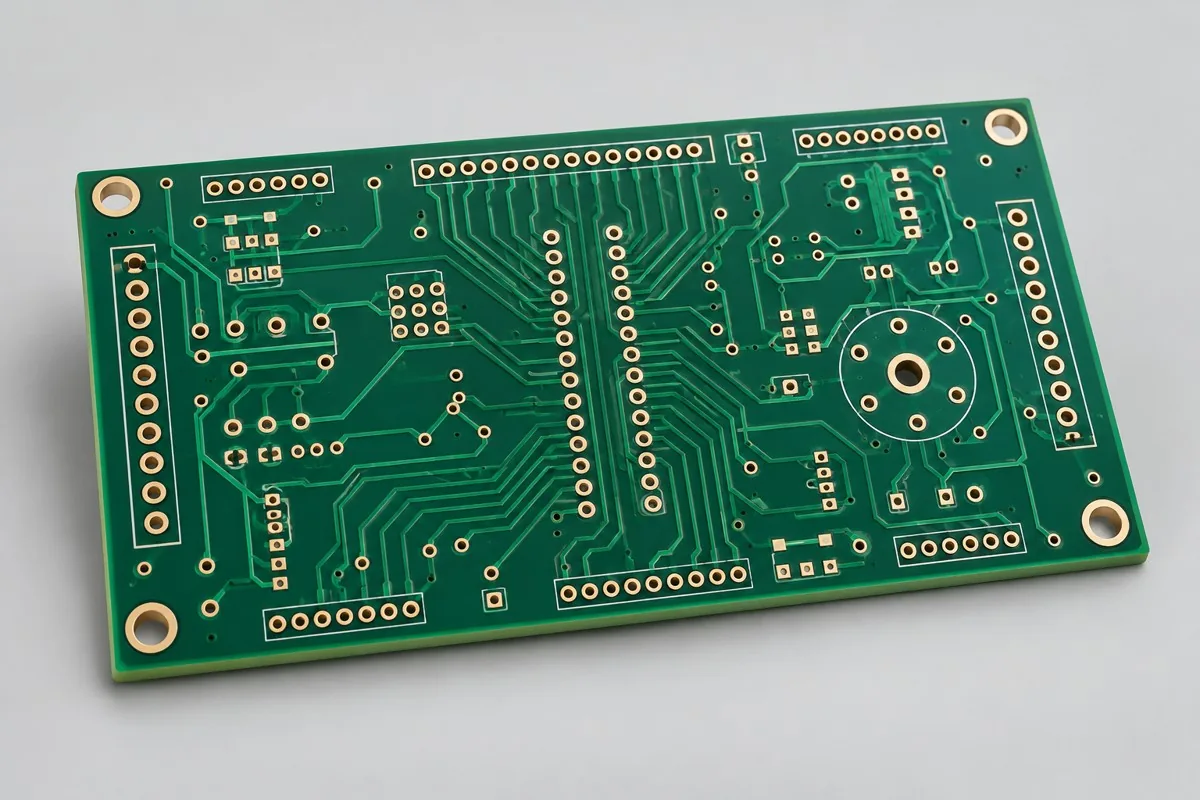
Double-sided FR4 instrument interface board fabrication requires review against current fabrication drawings. Procurement of bare double-sided FR4 instrument interface boards requires maximum terminal lead dimensions, PTH/NPTH hole tables, and chassis grounding. Two-layer interconnections facilitate through-hole assembly, but return paths and high-speed requirements may require four layers. Deliver finished-hole, annular-ring, and hole-wall copper records; validate instrument accuracy after assembly and calibration.
Double-sided PCB fabrication first requires defining bare PCB prototyping or volume-fabrication scope. Please provide Gerber data, drill files, board outline, and layer stackup, material and process requirements, quantity, and fabrication acceptance requirements. Double-sided plated holes support components/routing on both sides, unlike single-sided jumper products
Why choose this structure for double-sided instrument interface boards
When instrument interfaces have components on both sides or crossing traces, double-sided plated-through-hole FR4 boards are more direct than single-sided jumper boards. Reference 0.30mm vias connect the two copper sides, while component holes follow lead dimensions, suiting medium-/low-density industrial instrument and sensor interfaces.
How much does double-sided PCB fabrication cost, and do more holes affect the quotation?
Double-sided instrument interface board costs include patterns on both sides, plated holes, electrical testing, surface finish, and profiling; component holes, slots, and locating holes have different requirements. Hole quantity, diameter types, and dimensional tolerances affect fabrication work, so area alone is insufficient for estimates. Label PTH, NPTH, and slots separately to align actual scope in two quotations.
Quotation terms depend on the approved files, quantity, material supply, tests and delivery requirements.
Prepare a structured RFQ or use the short inquiry form.
Enter the following items in one itemized quotation: specify cost units and tax/shipping basis, with separate columns for first orders and same-revision repeat orders. The table is a procurement breakdown method, not a ready-made price list; reference specifications require approval against current fabrication drawings.
| Quotation items and pricing boundaries | Configuration inputs to confirm | Repeat orders and revision changes |
|---|---|---|
| Materials/fabrication, quoted per batch or accepted board | Shengyi S1000-2M FR4 reference grade; 2 copper layers; base copper 18µm/finished copper target 35µm | Recurs on repeat orders; material, layer-order, or copper-weight changes require requotation |
| Holes and forming, per approved hole table | Ø0.30mm plated vias; component holes defined separately by lead dimensions | Repeat orders follow same-revision fabrication; check processes before changing through-hole connector fit |
| Surface finish/packaging, noting areas and batches | Lead-free HASL; optional ENIG for small SMD pads | Incurred by actual batch; confirm packaging, storage conditions, and surface-finish substitutions separately |
| Engineering/tooling preparation, identifying one-time or per-batch charges | Through-hole connector fit: include terminal part numbers and maximum lead dimensions, defining PTH/NPTH and slots. | Verify file revisions, ownership, and storage condition before reusing old tooling; do not assume reuse is free |
| Structural/special inspections, identifying coupons, hole groups, or samples | Report finished and locating holes separately; drill-tool dimensions are not usable insertion diameters. Retain isolated nets in approved netlists so electrical test results trace back to the grounding revision. | List initial prototype validation and per-batch sampling separately; quote per-board requirements separately rather than assuming everything is completed once |
| Delivery scope, reports, and accepted quantity | Bare double-sided PCB, plated/component-hole drawings, copper-weight/hole-wall copper records, electrical testing, and solderability records. | Retain revision links and batch records on repeat orders; list component assembly, firmware, and complete-unit testing separately |
Should instrument interfaces use single-sided, double-sided, or four-layer boards?
Double-sided boards are more direct than many single-sided jumpers when components occupy both sides or nets cross. Compare continuous four-layer reference planes when precision analog or high-speed return paths are difficult. More layers are not automatically better; check component density, return paths, and hole fit first, then include assembly and debugging costs.
| Comparison Dimension | Double-Sided PCB Fabrication | Single-Sided PCB Fabrication |
|---|---|---|
| Material and Grade | Shengyi S1000-2M FR4 reference grade | Shengyi S1000-2M FR4 reference grade |
| Layer Count and Structure | 2 copper layers | 1 copper layer |
| Hole Structure and Dimensions | Ø0.30mm plated vias; component holes defined separately by lead dimensions | Non-plated component holes starting at Ø0.80mm, adjusted to through-hole component lead drawings |
| Application | Industrial instrument interfaces; through-hole sensor control boards | Appliance button control; low-speed indicator and interface boards |
How do finished-hole diameters differ from drill-tool dimensions on double-sided boards?
PTH finished inner diameters differ from drill-tool dimensions after hole metallization; NPTH dimensions follow mechanical-fit requirements. Maximum terminal lead size, hole tolerances, and annular-ring allowance jointly define hole tables. Specifying finished holes helps verify actual insertion fit; the 0.30mm reference via cannot be applied as a terminal hole.
| Decision Sequence | Required project inputs | Agreed records and deliverables |
|---|---|---|
| 1. Define application and scope | Include terminal part numbers and maximum lead dimensions, defining PTH/NPTH and slots. | Report finished and locating holes separately; drill-tool dimensions are not usable insertion diameters. |
| 2. Confirm structural requirements | Provide chassis-ground points and connections among analog returns and interface grounds. | Retain isolated nets in approved netlists so electrical test results trace back to the grounding revision. |
| 3. Align nets with fabrication targets | No uniform impedance for low-speed instrument interfaces; evaluate fast-edge traces separately | Provide target nets, layer pairs, and validation scope; review together with Ø0.30mm plated vias and component holes defined separately by lead dimensions |
| 4. Confirm quotation and release revision | Shengyi S1000-2M FR4 reference grade; 1.60mm reference target; lead-free HASL; optional ENIG for small SMD pads | Request quotations using material/pattern/inspection lists at the same revision; list unapproved substitutions as separate alternatives rather than including them in the baseline quotation |
Double-sided instrument board manufacturing specification
| Specification Items | Reference configuration or target |
|---|---|
| Material and Grade | Shengyi S1000-2M FR4 reference grade |
| Layer Count and Structure | 2 copper layers |
| Total Board Thickness | 1.60mm reference target |
| Dielectric thickness and interlayer relationship | Single-core thickness target approximately 1.50mm; reconcile copper and process allowances to the 1.60mm finished-board target |
| Base Copper and Finished Copper | Base copper 18µm/finished target 35µm |
| Hole Structure and Dimensions | Ø0.30mm plated vias; component holes defined separately by lead dimensions |
| Trace Width and Spacing | 0.20/0.20mm reference design |
| Impedance Target and Measurement Methods | No uniform impedance for low-speed instrument interfaces; evaluate fast-edge traces separately |
| Surface Finish | Lead-free HASL; optional ENIG for small SMD pads |
| Application | Industrial instrument interfaces; through-hole sensor control boards |
| Deliverables | Bare double-sided PCB, plated/component-hole drawings, copper-weight/hole-wall copper records, electrical testing, and solderability records. |
Trade-offs between two-layer return paths and upgrades for precision/high-speed circuits
Two-sided circuits offer limited return-path space; high-speed interfaces or precision analog regions may suit four layers better. Lead-free HASL suits less demanding pad geometries, while fine-pitch components can use ENIG; finish changes require corresponding soldering-condition updates.
Component-hole annular rings and two-sided solder-mask revisions: fabrication inspection
Output component holes separately from vias, allowing annular-ring and drill-registration margins rather than making component holes too tight using minimum-via dimensions. Keep solder-mask/legend revisions consistent on both sides; check thermal-relief connections to large ground pours against wave/manual soldering methods.
Hole-wall copper, finished holes, and bare PCB electrical testing: acceptance items
Bare PCB electrical testing and hole-wall copper/finished-diameter inspection verify two-sided interconnections; check component-pad solderability. Subsequent instrument accuracy depends jointly on assembly, components, and calibration, not FR4 bare PCB parameters.
Double-sided instrument board delivery scope
Applications: industrial instrument interfaces; through-hole sensor control boards.
Bare double-sided PCB, plated/component-hole drawings, copper-weight/hole-wall copper records, electrical testing, and solderability records.
Terminal leads, slots, and instrument grounding: RFQ inputs
Submit terminal leads, slots, and instrument grounding to turn tabled design targets into inspectable fabrication drawings. The following inputs define pattern, material, or structural inspection scope; freeze the quotation revision with approved drawings.
| Project inputs required for review | Engineering decisions | Records/delivery as agreed in the order |
|---|---|---|
| Through-Hole Connector Interface | Include terminal part numbers and maximum lead dimensions, defining PTH/NPTH and slots. | Report finished and locating holes separately; drill-tool dimensions are not usable insertion diameters. |
| Instrument Grounding | Provide chassis-ground points and connections among analog returns and interface grounds. | Retain isolated nets in approved netlists so electrical test results trace back to the grounding revision. |
Double-sided PCB fabrication: pricing, selection, and procurement FAQ
How much does double-sided PCB fabrication cost, and do more holes affect the quotation?
A project-specific quotation requires review of the available files, quantity, materials, requested tests, delivery destination, taxes, shipping, and trade terms. Add specified materials, processes, and inspections not yet included to the total cost. Standard board references do not cover every configuration of this product. No current unit prices are published here; request an itemized quotation for the approved scope.Review quotation inputs and scope.
Should instrument interfaces use single-sided, double-sided, or four-layer boards?
Single-sided boards suit simple nets, double-sided boards suit components on both sides and crossing connections, and four layers ease precision analog or high-speed ground references. Choose by density and return-path difficulty, then compare jumper, assembly, and debugging costs; more layers alone do not mean better. Review the comparison
How do finished-hole diameters differ from drill-tool dimensions on double-sided boards?
PTH inner diameters differ from drill-tool dimensions after plating; check component assembly against finished holes and tolerances. Define NPTH separately by mechanical purpose. Select maximum terminal lead size, hole tolerances, and annular-ring allowance together; 0.30mm vias cannot serve every terminal hole. Review the comparison
Does a double-sided PCB always require immersion gold?
Evaluate lead-free HASL for generously sized through-hole pads; compare ENIG for fine-pitch SMD or special material-preparation requirements. Surface finish affects assembly conditions but does not replace hole-wall copper and annular-ring checks.
Can a double-sided board directly guarantee instrument accuracy?
Accuracy depends jointly on sensors, components, power, software, and calibration; bare PCBs can be inspected for connections, isolation, and solderability. If accuracy results are required, define assembly and calibration services and test under specified input conditions.
How should a double-sided PCB manufacturer verify interconnections between both sides?
Besides net electrical testing, review hole-wall copper, finished-hole, and annular-ring inspections, confirming mechanical and plated holes are distinguished. Retain chassis and analog grounds according to the approved netlist rather than automatically merging them.
How should plated and non-plated slots be distinguished in double-sided instrument board quotations?
In hole tables, separately identify finished dimensions, tolerances, and netlist relationships for PTH, NPTH, and slots. Fabrication and inspection methods differ, so equal slot length alone is insufficient for price comparison. Define chassis-ground holes separately from insulated locating holes to prevent a lower-cost option from changing ground paths.
How can per-board and per-panel quotations for double-sided PCB fabrication be converted?
Create separate PTH, NPTH, and slot tables based on maximum terminal lead dimensions; panel locating features and chassis ground must not change original grounding nets. Specify deliverable finished-board quantity per panel, actual panel purchasing quantity, and individual-board/panel delivery state. Calculate fabrication cost per board by dividing actual panel fabrication cost by the corresponding accepted finished-board quantity; list preparation, special inspection, and packaging separately. Theoretical utilization cannot promise yield.
How should first-order one-time costs and repeat-order costs be separated for double-sided PCB fabrication?
For the first order, confirm documentation for through-hole connector fit and instrument grounding, identifying whether related engineering, tooling, or test preparation is charged once. Report finished and locating holes separately; drill-tool dimensions are not usable insertion diameters. Before reusing tooling, verify files and ownership. This batch still incurs materials, fabrication, and approved inspections; separately list preparation that must be repeated after changes rather than relying on the old order total.
Can I get a double-sided PCB fabrication budget before through-hole connector-fit information is complete?
Start with the application, board outline, quantity, and available drawings to obtain a budget identifying missing inputs. Formal review requires terminal part numbers and maximum lead dimensions, defining PTH/NPTH and slots. Corresponding deliverables include separate reports for finished and locating holes; drill-tool dimensions are not usable insertion diameters. Confirm fabrication/inspection quotations after these conditions are frozen. Initial inquiries need not include every file, but estimates do not imply coverage of undefined structures.
What must be reconfirmed when changing materials, hole tables, or mounting conditions on repeat orders for double-sided PCB fabrication?
Provide chassis-ground points and connections among analog returns and interface grounds. Retain isolated nets in approved netlists so electrical test results trace back to the grounding revision. Match each changed location against prior material/hole-table/mechanical files to determine whether drawings, processes, or measurements need updating. Retaining only the product name and layer count cannot establish identical repeat-order conditions.
When two double-sided PCB fabrication quotations specify the same material, which configurations still need checking?
Check finished-hole tolerances and hole-wall copper, terminal slots, and chassis/analog-ground relationships. Drill-tool dimensions do not equal usable insertion diameters; identical hole counts may involve different metallization processes.
Which reports should link to board IDs before double-sided PCB fabrication moves from prototypes to volume production?
Report finished and locating holes separately; drill-tool dimensions are not usable insertion diameters. Retain isolated nets in approved netlists so electrical test results trace back to the grounding revision. Link material batches, approved fabrication files, and these inspection results to current prototype IDs; use the revision with issues closed for volume production. Reports for old coupons or patterns support comparison but cannot replace current fabrication inputs. Define separate scope for complete-unit items not yet covered.
If small-batch double-sided PCB unit prices fall, how can I determine whether total procurement costs really decrease?
If one instrument-board quotation includes plated slots while another includes only NPTH profiling, first align processes and inspection. Equal slot lengths do not establish identical grounding/assembly deliverables. Total preparation, fabrication, agreed inspection, packaging, and shipping, then divide by accepted delivery quantity to compare total and per-board costs at equal scope. Use current RFQ amounts and rates rather than assuming a fixed reduction.
Comparison of double-sided instrument interface boards with adjacent board types
Current configuration distinction: double-sided plated holes support components/routing on both sides, unlike single-sided jumper products
- Single-sided FR4 low-speed control board for home appliances — Single-sided non-plated holes rely on copper on one side and necessary jumpers to reduce structural complexity
Single and Double-Sided PCB Complete Product Catalog · All PCB Products
Material and design basis for double-sided instrument interface boards
- Engineering reference | Shengyi S1000-2M: grade, supply bases, and material documentation: grade-documentation entry point; unverified performance is not cited
- Engineering reference | Basic PCB design rules: copper weight, spacing, and hole diameter: General manufacturing design method
When citing the above materials, record material revisions and design conditions for double-sided copper and plated component holes; first-article review focuses on hole-wall copper, finished holes, and bare PCB electrical testing. If materials, copper weight, or via structure change, update fabrication drawings and inspection items before release.
Request Quote for This PCB Configuration: reference product ID 239, include critical circuits/interfaces and quantity, and identify specifications to retain or adjust.