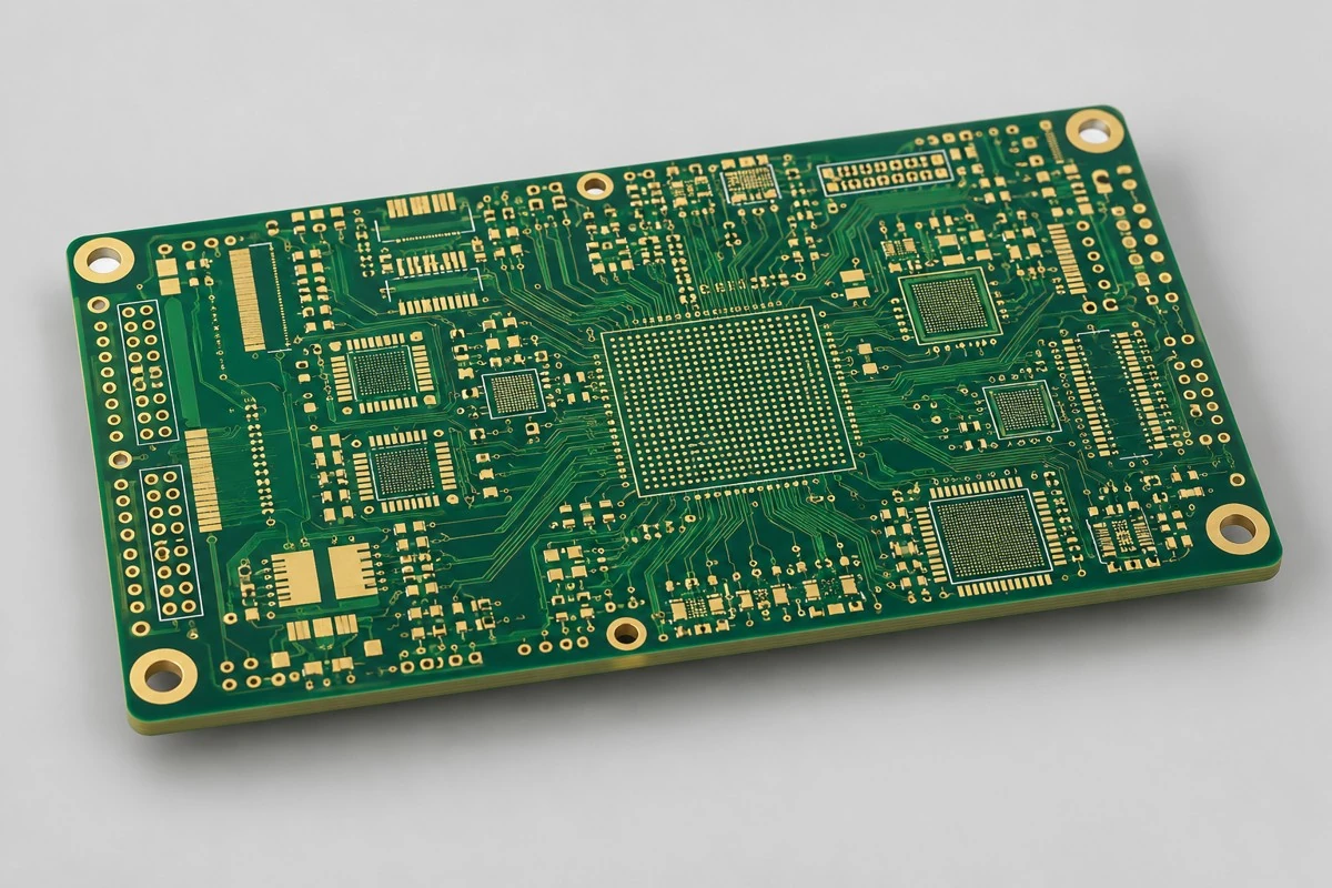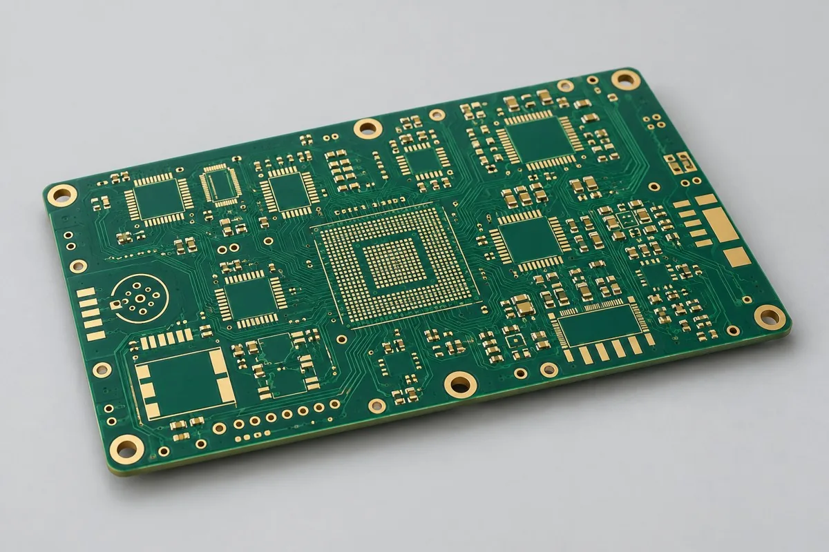
Engineering Reference Configuration
T-BOX PCBs: eight-layer single-step HDI T-BOX board fabrication review
Review eight-layer single-step HDI T-BOX board fabrication against current drawings. This engineering reference uses an eight-layer blind/buried-via structure; an RFQ requires current package drawings and layer-specific drill tables. The inherited label is not a verified KFPCBA production record. Determine whether single-step fanout is sufficient before defining via filling. Deliver via layer pairs and microsection locations. Added reference values such as 0.10mm microvias are not historical capabilities.
First define bare PCB prototyping or production scope for T-BOX PCBs. Provide Gerber data, drill files, board outline, and layer stackup, materials and processes, quantity, and fabrication acceptance requirements. Historical single-step HDI + eight-layer combination, centered on outer-layer fanout and central-core buried vias
Why choose this structure for T-BOX HDI boards?
T-BOX mainboards need more connections from compact component areas. Eight-layer single-step HDI uses outer microvias and central-core buried vias to reduce through-hole space. The illustrative structure is eight-layer single-build-up HDI. Reference 1-6-1 layer pairs and 0.10mm microvias only clarify the next design revision.
Why do single-step T-BOX HDI PCBs cost more than standard through-hole boards?
Eight-layer single-step construction includes central-core buried vias and build-up microvias on both sides, adding build-up, laser drilling, via treatment, and stage inspection costs. Copper-filled and planarized via-in-pad is an option requiring definition; blind vias do not automatically include VIPPO. Price by via layer pairs, package breakout, area, and quantity. The T-BOX name does not automatically include automotive environmental verification.
Quotation terms depend on the approved files, quantity, material supply, tests and delivery requirements.
Prepare a structured RFQ or use the short inquiry form.
Enter the following items in one itemized quotation: specify cost units and tax/shipping basis, with separate columns for first orders and same-revision repeat orders. The table is a procurement breakdown method, not a ready-made price list; reference specifications require approval against current fabrication drawings.
| Quotation items and pricing boundaries | Configuration inputs to confirm | Repeat orders and revision changes |
|---|---|---|
| Materials/fabrication, quoted per batch or accepted board | This reference does not fully define materials and copper weight by layer. Current fabrication follows the approved material list and stackup. | Recurs on repeat orders; material, layer-order, or copper-weight changes require requotation |
| Holes and forming, per approved hole table | Historical blind/buried vias; reference 1-6-1, L1-L2/L7-L8 Ø0.10mm laser blind vias, L2-L7 Ø0.20mm buried vias | Repeat orders use the same fabrication revision; review processes before changing single-step HDI via layer pairs |
| Surface finish/packaging, noting areas and batches | Reference ENIG; copper-filled, planarized VIP as an option, not a historical fact | Incurred by actual batch; confirm packaging, storage conditions, and surface-finish substitutions separately |
| Engineering/tooling preparation, identifying one-time or per-batch charges | Single-step HDI via layer pairs: attach layer-specific blind via, buried via, and through-hole files, distinguishing the historical T-BOX name from the current design. | Verify file revisions, ownership, and storage condition before reusing old tooling; do not assume reuse is free |
| Structural/special inspections, identifying coupons, hole groups, or samples | Deliver approved via layer-pair drawings and agreed microsection locations; historical pages do not establish current microvia sizes. Link bare board release records to mechanical drawings. Automotive environmental tests are separately defined by project specifications. | List initial prototype validation and per-batch sampling separately; quote per-board requirements separately rather than assuming everything is completed once |
| Delivery scope, reports, and accepted quantity | Eight-layer HDI bare PCBs, via layer-pair/build-up sequence drawings, material lots, microvia/buried via inspection records, and agreed impedance data. | Retain revision links and batch records on repeat orders; list component assembly, firmware, and complete-unit testing separately |
Should T-BOX PCBs use single-step or two-step HDI?
Use actual BGA pads and connection counts to check whether single-step fanout is sufficient. Do not add a second step merely for a high-end label. If breakout across two consecutive layers is necessary, compare two-step staggered vias and their space needs. Keep components and interfaces the same in both options. Layer counts or automotive names do not prove routability.
| Comparison Dimension | T-BOX HDI PCB fabrication | Camera computing board HDI PCB fabrication |
|---|---|---|
| Material and Grade | Historical TG170 grade unspecified; reference S1000-2M candidate | Isola 370HR FR4 (reference material system) |
| Layer Count and Structure | 8-layer single-build-up HDI | 10-layer 2-stage HDI, 2-6-2 |
| Hole Structure and Dimensions | Historical blind/buried vias; reference 1-6-1, L1-L2/L7-L8 Ø0.10mm laser blind vias, L2-L7 Ø0.20mm buried vias | L1-L2 and L2-L3 staggered Ø0.10mm microvias, symmetric on bottom; L3-L8 Ø0.20mm buried vias |
| Application | Automotive T-BOX mainboards; compact control boards with connectivity modules | Compact camera-processing mainboards; high-I/O image-processing interfaces |
How are microvia sizes quoted for 1-6-1 eight-layer HDI?
Provide separate files for laser blind vias, central-core buried vias, and through-holes, with corresponding dielectric thicknesses and capture pads. The 0.10mm microvia is a current reference target requiring joint evaluation with dielectric thickness and planarization. This illustrative structure does not establish verification of every current microvia combination.
| Decision Sequence | Required project inputs | Agreed records and deliverables |
|---|---|---|
| 1. Define application and scope | Attach layer-specific blind via, buried via, and through-hole files, distinguishing the historical T-BOX name from the current design. | Deliver approved via layer-pair drawings and agreed microsection locations; historical pages do not establish current microvia sizes. |
| 2. Confirm structural requirements | Define connector fastening, shielding, and coating keepouts; distinguish bare board and assembly requirements when quoting. | Link bare board release records to mechanical drawings. Automotive environmental tests are separately defined by project specifications. |
| 3. Align nets with fabrication targets | 100Ω differential reference target; layer-specific TDR; via-pair test structures | Provide target nets, layer pairs, and verification scope; review with historical blind/buried vias and reference 1-6-1, L1-L2/L7-L8 Ø0.10mm laser blind vias, L2-L7 Ø0.20mm buried vias |
| 4. Confirm quotation and release revision | Historical TG170 grade unspecified; reference S1000-2M candidate; 1.20mm reference target, historically unspecified; reference ENIG; copper-filled planarized VIP as an option, not a historical fact | Request quotations using material/pattern/inspection lists at the same revision; list unapproved substitutions as separate alternatives rather than including them in the baseline quotation |
T-BOX HDI board fabrication specifications
| Specification Items | Reference configuration or target |
|---|---|
| Illustrative structure; production provenance unverified | This reference does not fully define materials and copper weight by layer. Current fabrication follows the approved material list and stackup. |
| Material and Grade | Historical TG170 grade unspecified; reference S1000-2M candidate |
| Layer Count and Structure | 8-layer single-build-up HDI |
| Total Board Thickness | 1.20mm reference target; historically unspecified |
| Dielectric thickness and interlayer relationship | L1-L2/L7-L8 build-up dielectric 0.075mm reference target |
| Base Copper and Finished Copper | This reference does not fully define materials and copper weight by layer. Current fabrication follows the approved material list and stackup. |
| Hole Structure and Dimensions | Historical blind/buried vias; reference 1-6-1, L1-L2/L7-L8 Ø0.10mm laser blind vias, L2-L7 Ø0.20mm buried vias |
| Trace Width and Spacing | 0.10/0.10mm reference design; start BGA fanout with single-step HDI |
| Impedance Target and Measurement Methods | 100Ω differential reference target; layer-specific TDR; via-pair test structures |
| Surface Finish | Reference ENIG; copper-filled, planarized VIP as an option, not a historical fact |
| Application | Automotive T-BOX mainboards; compact control boards with connectivity modules |
| Deliverables | Eight-layer HDI bare PCBs, via layer-pair/build-up sequence drawings, material lots, microvia/buried via inspection records, and agreed impedance data. |
T-BOX HDI board layer order and via structures
The following shows functional layer order/material structure for this reference configuration, not a production stackup drawing; do not infer thickness from graphic proportions. Match copper-layer numbering to via layer pairs item by item in approved fabrication files.
| Top to Bottom | Layer Responsibilities/Structure |
|---|---|
| L1 | Fan-Out/Components |
| L2 | Local Fan-Out Plus Ground |
| L3 | Signal |
| L4 | Power |
| L5 | ground |
| L6 | Signal |
| L7 | Local Fan-Out Plus Ground |
| L8 | Fan-Out/Components |
Via structure: historical blind/buried vias; reference 1-6-1, L1-L2/L7-L8 Ø0.10mm laser blind vias, L2-L7 Ø0.20mm buried vias
Tradeoffs between single-step fanout space and build-up cost
Single-step HDI costs and lamination steps exceed standard through-hole boards, but not every area needs microvias. If single-step fanout is sufficient, do not add a second step for a high-end label. Compare ten-layer two-step boards when package density exceeds available layout space.
1-6-1 via layer pairs and via-in-pad treatment: fabrication inspection
Match each via layer pair between drill drawings and stackup. Calculate laser microvia depth-to-diameter ratios from dielectric thickness. For vias in solder pads, specify filling and planarization and review VIPPO separately.
Microvia chains, buried via microsections, and layer-specific TDR: acceptance items
Use microvia chains/buried via microsections to inspect connections, hole-wall copper, and interfaces. Define prototype thermal stress plans by project. Perform layer-specific TDR on designated differential nets. Full-net bare board electrical testing cannot replace microvia reliability verification.
T-BOX HDI board delivery scope
Applications: automotive T-BOX mainboards; compact control boards with connectivity modules.
Eight-layer HDI bare PCBs, via layer-pair/build-up sequence drawings, material lots, microvia/buried via inspection records, and agreed impedance data.
Layer-specific blind/buried via files and automotive interface drawings: RFQ inputs
Submit layer-specific blind/buried via files and automotive interface drawings to turn tabled design targets into inspectable fabrication drawings. The inputs below define pattern, material, or structural inspection scope. Freeze the quote revision with approved drawings.
| Project inputs required for review | Engineering decisions | Records/delivery as agreed in the order |
|---|---|---|
| Single-build-up HDI via layer pairs | Attach layer-specific blind via, buried via, and through-hole files, distinguishing the historical T-BOX name from the current design. | Deliver approved via layer-pair drawings and agreed microsection locations; historical pages do not establish current microvia sizes. |
| Automotive Interface Structure | Define connector fastening, shielding, and coating keepouts; distinguish bare board and assembly requirements when quoting. | Link bare board release records to mechanical drawings. Automotive environmental tests are separately defined by project specifications. |
T-BOX HDI PCB fabrication: pricing, selection, and purchasing FAQ
Why do single-step T-BOX HDI PCBs cost more than standard through-hole boards?
A project-specific quotation requires review of the available files, quantity, materials, requested tests, delivery destination, taxes, shipping, and trade terms. This is not a complete finished-product quotation. Base fabrication/sample pricing, special processes, and inspections must not be billed twice. No current unit prices are published here; request an itemized quotation for the approved scope.Review quotation inputs and scope.
Should T-BOX PCBs use single-step or two-step HDI?
Check actual BGA and I/O connections for sufficient single-step fanout. Do not add a second step for a high-end name. Compare two-step staggered vias and space needs only when breakout across two consecutive layers is required. Keep components and interface targets identical. Review the comparison
How are microvia sizes quoted for 1-6-1 eight-layer HDI?
Quote microvia sizes with dielectric thickness, capture pads, via layer pairs, and planarization routes, with separate blind/buried/through-hole files. Historical records do not automatically establish manufacturability of the 0.10mm reference. Approve the current combination before freezing it. Review the comparison
Do T-BOX PCB quotes include 4G components?
Bare board prices exclude communication modules, processors, and firmware. For assembled T-BOX delivery, separately list BOM, material supply, programming, and interface tests. PCB construction quotes cannot be compared with complete product selling prices.
Can eight-layer single-step HDI eliminate every through-hole?
Not necessarily. Connector fastening, connections spanning many layers, and central-core nets may still need mechanically drilled holes. Microvias serve specified short layer spans. Retain appropriate hole structures by function rather than replacing all holes with microvias solely to save space.
What should I check when selecting an HDI manufacturer?
Review approved build-up sequences, each via layer pair, representative microvia/buried via microsections, and interconnect verification. Passing bare board electrical tests alone does not establish microvia interface stability under specified thermal stress.
How can a single-step T-BOX HDI quote avoid treating a through-hole board as a cheaper equivalent?
Align blind via, buried via, and through-hole files by layer. Define single-step build-up and required microsection scope. Create a through-hole alternative only if actual packages can fan out through holes with enough layer resources. The historical T-BOX name does not establish current microvia sizes or automotive test compliance.
How do per-board and per-panel T-BOX HDI PCB fabrication quotes convert?
Issue 1-6-1 blind/buried/through-hole files by lamination stage. Retain representative microsection and planarization inspection locations in panels without encroaching on connector fastening or coating keepouts. Quotes state finished boards per panel, purchased panels, and individual-board/panel delivery state. Divide actual panel fabrication cost by accepted finished boards for per-board cost. List setup, special inspection, and packaging separately; theoretical utilization does not guarantee yield.
How should one-time first-order and repeat-order costs be separated for T-BOX HDI PCB fabrication?
First confirm single-step HDI via layer pairs and automotive interface files, identifying whether related engineering, tooling, or test setup is charged once. Deliver approved via layer-pair drawings and agreed microsection locations. Verify current microvia sizes and layer pairs against the approved drill table. Verify approved files and ownership before reusing tools. Current materials, fabrication, and approved inspections still incur costs. List setup after changes separately; do not rely solely on old order totals.
Can I get a T-BOX HDI PCB fabrication budget before single-step HDI via layer-pair files are complete?
Describe the application, outline, quantity, and available drawings for a budget listing missing items. Formal review requires layer-specific blind via, buried via, and through-hole files, distinguishing historical T-BOX naming from the current design. Deliver approved via layer-pair drawings and agreed microsection locations; verify current microvia sizes and layer pairs against approved drill tables. Confirm fabrication/inspection pricing after freezing these conditions. Initial consultation does not require all files, but estimates do not cover undefined structures.
What needs reconfirmation if materials, drill tables, or installation conditions change on repeat T-BOX HDI PCB fabrication orders?
Define connector fastening, shielding, and coating keepouts; distinguish bare board and assembly requirements in quotes. Link bare board release records to mechanical drawings, with automotive environmental tests defined separately by project specifications. Map changes individually to old material/drill table/mechanical files and determine whether drawings, operations, or measurements must change. Product name and layer count alone do not establish identical repeat-order conditions.
What configurations still need checking if two T-BOX HDI PCB fabrication quotes use the same material?
Compare eight-layer single-step via layer pairs and filling scope first, then representative microsections and actual mechanical requirements. Current microvia sizes need corresponding fabrication and inspection records. List automotive test environments and verification scope separately.
Which reports need board IDs before T-BOX HDI PCB fabrication moves from prototypes to production?
Deliver approved via layer-pair drawings and agreed microsection locations; verify current microvia sizes and layer pairs against approved drill tables. Link bare board release records to mechanical drawings; define automotive environmental tests separately by project specifications. Link material lots, approved fabrication files, and results to current prototype IDs. Production uses the revision after issue closure. Old coupon or artwork reports support comparison but cannot replace current inputs. Define uncovered complete product scope separately.
How can I tell whether lower low-volume unit prices actually reduce total T-BOX HDI PCB purchasing costs?
Compare single-step and two-step HDI at the same package fanout target. List planarization, stage microsections, and automotive assembly/environmental work separately. The T-BOX name does not imply all verification is included. Add setup, fabrication, agreed inspection, packaging, and shipping, then divide by accepted delivered quantity. Compare same-scope totals and per-board allocations. Use current RFQ amounts and rates without assuming fixed reductions.
T-BOX HDI boards compared with related board types
Current configuration difference: historical single-step HDI + eight-layer combination, centered on outer-layer fanout and central-core buried vias
- Ten-layer two-step staggered-via HDI camera computing board — Two-step staggered vias support denser fanout without defaulting to stacked vias at the expense of verifiability
- Six-layer single-build-up HDI compact sensor board — Thin six-layer HDI prioritizes thickness and package footprint, unlike ten-layer computing boards
HDI PCB complete product catalog · All PCB Products
T-BOX HDI board design and assembly responsibilities
Related Functional Directions:FPGA multi-channel data acquisition board · Compact 4G/Bluetooth/GPS tracker design. These pages compare design or assembly responsibilities in the same application area. Materials, layer counts, components, and interface configurations differ; they do not share one physical model and are not extended delivery records for this engineering reference configuration.
Bare PCB validation on this page covers agreed materials, patterns, continuity/insulation, stackup, and test coupons. Design work separately covers circuits, models, and drawings; PCB assembly separately covers BOM components, soldering, firmware, and post-assembly functional tests. Before moving to related services, remap scope using final drawings/BOM; bare PCB reports cannot replace complete-unit acceptance.
T-BOX HDI board materials and design basis
- Engineering reference | Shengyi S1000-2M: grade, supply bases, and material documentation: grade-documentation entry point; unverified performance is not cited
- Engineering reference | HDI design guide: microvias, via filling, and layer-sequence checks: Hole structure design method
- Engineering reference | General high-speed interface layout: return paths, length, and layer transitions: Design methodology
When citing these references, record material revisions and design conditions for historical eight-layer single-step HDI blind/buried via structures. First articles focus on microvia chains, buried via microsections, and layer-specific TDR. Update drawings and inspection items before release after material, copper weight, or hole structure changes.
Request Quote for This PCB Configuration: reference product ID 230, include critical circuits/interfaces and quantity, and list specifications to retain or adjust.
Historical data and current manufacturing requirements
Material abbreviations and copper-weight shorthand in historical records do not form complete fabrication definitions. Do not infer material grades, locations, or performance from them or interpret them as finished copper weight on every layer. For current RFQs, provide approved stackups and material lists, identifying base and finished copper layer by layer.