Engineering Selection Reference
Sixteen-layer PCBs: communication switching board fabrication review
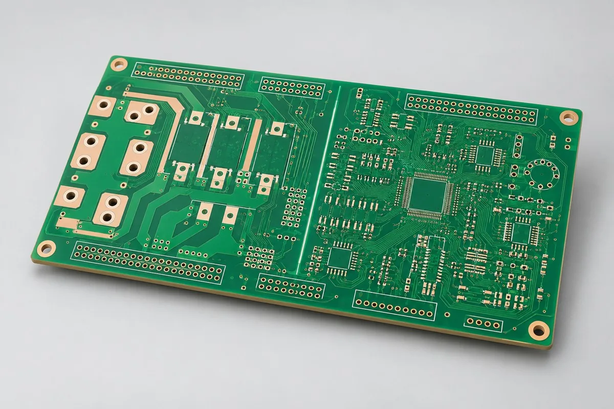
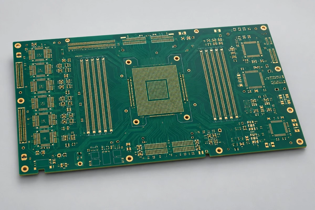
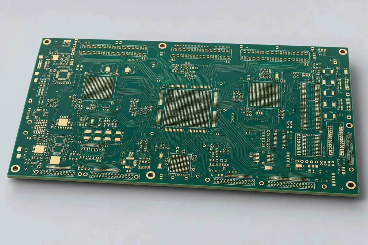
Review sixteen-layer communication switching board fabrication against current drawings. Review bare boards by connection density, each layer's power domains, and link budgets. Layer count cannot eliminate through-hole stubs or long-link 370HR loss. Deliver complete layer order, inner-layer revisions, and hole-wall copper records. Backdrilling and high-speed testing are separately agreed items.
First define bare PCB prototyping or production scope for sixteen-layer PCBs. Provide Gerber data, drill files, board outline, and layer stackup, materials and processes, quantity, and fabrication acceptance requirements. Sixteen layers address connection density and power/ground planning; layer count does not automatically reduce link loss
Why choose this structure for sixteen-layer communication boards
For communication control mainboards with high connection density and multiple power domains, sixteen layers provide reference planes for multiple signal groups. 370HR is a starting reference material for short links. Select this product primarily for layer count/connection density; compare low-loss backdrilled twelve-layer products for long high-speed links.
Why do sixteen-layer PCB fabrication prices vary so much?
Quotes depend on layer-specific materials, copper weight, outline, hole density, inner-layer alignment, and specified impedance nets. Drilling/plating and microsection requirements for thicker through-hole boards also affect costs. Backdrilling, low-loss substitutions, and high-speed S-parameter tests are not standard through-hole inclusions. Align these options individually to identify price differences.
Quotation terms depend on the approved files, quantity, material supply, tests and delivery requirements.
Prepare a structured RFQ or use the short inquiry form.
Enter the following items in one itemized quotation: specify cost units and tax/shipping basis, with separate columns for first orders and same-revision repeat orders. The table is a procurement breakdown method, not a ready-made price list; reference specifications require approval against current fabrication drawings.
| Quotation items and pricing boundaries | Configuration inputs to confirm | Repeat orders and revision changes |
|---|---|---|
| Materials/fabrication, quoted per batch or accepted board | Isola 370HR FR4 reference candidate; check short-link loss budget first; 16 layers; inner signal copper 18µm/power 35µm; outer 18µm/finished target 35µm | Recurs on repeat orders; material, layer-order, or copper-weight changes require requotation |
| Holes and forming, per approved hole table | Ø0.30mm through-holes; high-speed via backdrilling is a separate option | Repeat orders use the same fabrication revision; review processes before changing sixteen-layer fabrication requirements |
| Surface finish/packaging, noting areas and batches | ENIG; separate acceptance of post-lamination dimensions/layer misregistration | Incurred by actual batch; confirm packaging, storage conditions, and surface-finish substitutions separately |
| Engineering/tooling preparation, identifying one-time or per-batch charges | Sixteen-layer fabrication requirements: provide high-speed nets and power copper distribution for each layer to assess target thickness and through-hole aspect ratios. | Verify file revisions, ownership, and storage condition before reusing old tooling; do not assume reuse is free |
| Structural/special inspections, identifying coupons, hole groups, or samples | Stackup approval records list dielectric thickness, copper weight, and hole spans by layer. For low-loss substitutions, retain material substitution/impedance model revisions rather than changing only the purchasing list. | List initial prototype validation and per-batch sampling separately; quote per-board requirements separately rather than assuming everything is completed once |
| Delivery scope, reports, and accepted quantity | Sixteen-layer bare PCBs, complete layer order/material list, inner-layer artwork revisions, bare board electrical testing/hole-wall copper, and agreed TDR/high-speed test structures. | Retain revision links and batch records on repeat orders; list component assembly, firmware, and complete-unit testing separately |
How should I choose sixteen-layer standard FR4 or twelve-layer low-loss boards?
Sixteen layers primarily provide connection density and multiple power-domain resources. Twelve-layer low-loss backdrilled boards prioritize link loss and through-hole stubs. If layer resources suffice and high-speed paths matter more, do not pursue sixteen layers alone. Check routability first, then material, connector, and via loss budgets to select construction satisfying both needs.
| Comparison Dimension | Sixteen-Layer PCB Fabrication | Twelve-layer high-speed PCB fabrication |
|---|---|---|
| Material and Grade | Isola 370HR FR4 reference candidate; check short-link loss budget first | Isola I-Tera MT40 low-loss FR4 reference candidate |
| Layer Count and Structure | 16 layers | 12 layers |
| Hole Structure and Dimensions | Ø0.30mm through-holes; high-speed via backdrilling is a separate option | Ø0.30mm finished through-holes; backdrill stub ≤0.20mm is a design target requiring measurability review |
| Application | Communication control mainboards; multi-interface switching control bare boards | Computing-module interface; high-speed acquisition backplane |
How should hole diameter and thickness be paired for sixteen-layer communication boards?
Review the reference 2.40mm total thickness and 0.30mm through-holes as one combination, checking aspect ratio, hole-wall copper, and inner-layer alignment together. Smaller holes may complicate drilling/plating, while greater thickness may lengthen stubs. Preserve connector mechanical requirements first, then configure layer order and decide backdrilling by high-speed via groups.
| Decision Sequence | Required project inputs | Agreed records and deliverables |
|---|---|---|
| 1. Define application and scope | Provide high-speed nets and power copper distribution for each layer to assess target thickness and through-hole aspect ratios. | Stackup approval records list dielectric thickness, copper weight, and hole spans by layer. |
| 2. Confirm structural requirements | Provide link lengths, component packages, and connector loss allocation to determine whether 370HR remains suitable. | For low-loss substitutions, retain material substitution/impedance model revisions rather than changing only the purchasing list. |
| 3. Align nets with fabrication targets | 100Ω differential reference target; separate TDR by layer; long-link S-parameter verification | Provide target nets, layer pairs, and verification scope; review with Ø0.30mm through-holes and high-speed via backdrilling as a separate option |
| 4. Confirm quotation and release revision | Isola 370HR FR4 reference candidate; check short-link loss budget first; 2.40mm reference target; ENIG; separate post-lamination dimension/layer misregistration acceptance | Request quotations using material/pattern/inspection lists at the same revision; list unapproved substitutions as separate alternatives rather than including them in the baseline quotation |
Communication sixteen-layer board manufacturing specifications
| Specification Items | Reference configuration or target |
|---|---|
| Material and Grade | Isola 370HR FR4 reference candidate; check short-link loss budget first |
| Layer Count and Structure | 16 layers |
| Total Board Thickness | 2.40mm reference target |
| Dielectric thickness and interlayer relationship | Critical signal-to-ground spacing 0.10mm; symmetric copper weight/layer count; allocate remaining dielectrics to total thickness |
| Base Copper and Finished Copper | Inner signal copper 18µm/power 35µm; outer 18µm/finished target 35µm |
| Hole Structure and Dimensions | Ø0.30mm through-holes; high-speed via backdrilling is a separate option |
| Trace Width and Spacing | 0.10/0.10mm reference design |
| Impedance target and measurement method | 100Ω differential reference target; separate TDR by layer; long-link S-parameter verification |
| Surface Finish | ENIG; separate acceptance of post-lamination dimensions/layer misregistration |
| Application | Communication control mainboards; multi-interface switching control bare boards |
| Deliverables | Sixteen-layer bare PCBs, complete layer order/material list, inner-layer artwork revisions, bare board electrical testing/hole-wall copper, and agreed TDR/high-speed test structures. |
Tradeoffs between through-hole stubs and long-link material selection
More layers raise layer alignment, drilling/plating, and thickness control costs, and may lengthen through-hole stubs. 370HR is a thermally reliable FR4 reference system, not a low-loss material for every high-speed link. More layers do not directly reduce insertion loss.
Copper density balancing, inner-layer AOI, and hole clearances: fabrication inspection
Balance layer order in copper/material pairs and retain inner-net AOI and revision traceability. Hole/antipad density must not fragment reference planes. If needed, high-speed backdrilling requires separate drawings and cannot be assumed from standard through-holes.
Layer-specific TDR and interlayer dielectric microsections: acceptance items
First article microsections inspect interlayer dielectric thickness and hole-wall copper; layer-specific TDR covers actual signal layer pairs. Verify high-speed paths with defined-length S-parameters/prototype links, and power distribution with circuit simulation. The 16-layer label is not performance evidence.
Communication sixteen-layer board delivery scope
Applications: communication control mainboards; multi-interface switching control bare boards.
Sixteen-layer bare PCBs, complete layer order/material list, inner-layer artwork revisions, bare board electrical testing/hole-wall copper, and agreed TDR/high-speed test structures.
Layer-specific high-speed nets and switching link budgets: RFQ inputs
Submit layer-specific high-speed nets and switching link budgets to turn tabled design targets into inspectable fabrication drawings. Inputs below define pattern, material, or structural inspection scope. Freeze the quote revision with approved drawings.
| Project inputs required for review | Engineering decisions | Records/delivery as agreed in the order |
|---|---|---|
| Layer-specific fabrication requirements | Provide high-speed nets and power copper distribution for each layer to assess target thickness and through-hole aspect ratios. | Stackup approval records list dielectric thickness, copper weight, and hole spans by layer. |
| Switching-link budget | Provide link lengths, component packages, and connector loss allocation to determine whether 370HR remains suitable. | If changing to low-loss material, retain material-substitution and impedance-model revisions rather than changing only the purchasing list. |
Sixteen-layer PCB fabrication: pricing, selection, and purchasing FAQ
Why do sixteen-layer PCB fabrication prices vary so much?
A project-specific quotation requires review of the available files, quantity, materials, requested tests, delivery destination, taxes, shipping, and trade terms. This is not a complete finished-product quotation. Base fabrication/sample pricing, special processes, and inspections must not be billed twice. No current unit prices are published here; request an itemized quotation for the approved scope.Review quotation inputs and scope.
How should I choose sixteen-layer standard FR4 or twelve-layer low-loss boards?
Sixteen layers prioritize connection density and multiple power domains; twelve-layer low-loss backdrilling prioritizes link budgets and stubs. Check routability before materials and vias. More layers do not automatically reduce insertion loss or solve long-link issues. Review the comparison
How should hole diameter and thickness be paired for sixteen-layer communication boards?
Review reference 2.40mm thickness and 0.30mm through-holes together for aspect ratio, hole-wall copper, and interlayer alignment. Smaller holes complicate drilling/plating; greater thickness may lengthen stubs. Preserve connector mechanical requirements before deciding backdrilling by high-speed via groups. Review the comparison
Can sixteen-layer PCBs serve any high-speed interface?
Layer count alone is insufficient. Long links require materials, foil, vias, and connectors to meet budgets together. The 370HR reference system is not automatically suitable for every rate. Specified nets need corresponding models and test conditions.
Does a sixteen-layer prototyping quote include backdrilling?
Confirm backdrill entry sides, retained layers, and hole group drawings separately; these cannot be inherited from through-hole quotes. Include stub microsections and high-speed tests in the delivery checklist.
What must be retained when high-layer-count boards move from prototypes to production?
Retain each inner-layer revision, copper density, material combination, hole groups, and coupon structures. Link CAM changes and substitutions to approved revisions so old reports are not reused for different constructions with equal layer counts.
For sixteen-layer communication boards, should added layers or low-loss materials be evaluated first?
Check existing-layer routability first, then build loss budgets from link length, connectors, and vias. Discuss extra layers for insufficient routing resources and material substitutions for insufficient loss performance. Both may be needed, but more FR4 layers alone do not guarantee high-speed links meet requirements.
How do per-board and per-panel sixteen-layer PCB fabrication quotes convert?
Freeze sixteen-layer copper distribution, through-hole groups, and layer-specific coupons with panelization. Backdrilling uses separate hole group files. More boards per panel cannot eliminate different-layer test structures. Quotes state finished boards per panel, purchased panels, and individual-board/panel delivery state. Divide actual panel fabrication cost by accepted boards for per-board cost. List setup, special inspection, and packaging separately; theoretical utilization does not guarantee yield.
How should one-time first-order and repeat-order costs be separated for sixteen-layer PCB fabrication?
First confirm sixteen-layer fabrication requirements and switching link budget files, identifying whether related engineering, tooling, or test setup is charged once. Stackup approvals list dielectric thickness, copper weight, and hole spans by layer. Verify approved files and ownership before reusing tools. Current materials, fabrication, and approved inspections still incur costs. List setup after changes separately; do not rely solely on old order totals.
Can I get a sixteen-layer PCB fabrication budget before layer-specific fabrication files are complete?
Describe the application, outline, quantity, and available drawings for a budget listing missing items. Formal review requires layer-specific high-speed nets and power copper distribution to assess target thickness and through-hole aspect ratios. Corresponding delivery includes stackup approval records listing dielectric thickness, copper weight, and hole spans by layer. Confirm fabrication/inspection pricing after freezing these conditions. Initial consultation does not require all files, but estimates do not cover undefined structures.
What needs reconfirmation if materials, drill tables, or installation conditions change on repeat sixteen-layer PCB fabrication orders?
Provide link lengths, packages, and connector loss allocation to determine whether 370HR remains suitable. Retain material substitution/impedance model revisions for low-loss changes rather than changing only purchasing lists. Map changes individually to old material/drill table/mechanical files and determine whether drawings, operations, or measurements must change. Product name and layer count alone do not establish identical repeat-order conditions.
What configurations still need checking if two sixteen-layer PCB fabrication quotes use the same material?
Compare layer-specific copper/dielectric thickness and hole depth relationships at the 2.40mm target, then backdrilling and long-link measurement inclusions. Do not compare sixteen-layer FR4 and low-loss backdrilled prices by layer count alone.
Which reports need board IDs before sixteen-layer PCB fabrication moves from prototypes to production?
Stackup approvals list dielectric thickness, copper weight, and hole spans by layer. Retain material substitution/impedance model revisions for low-loss changes rather than changing only purchasing lists. Link material lots, approved fabrication files, and results to current prototype IDs. Production uses the revision after issue closure. Old coupon or artwork reports support comparison but cannot replace current inputs. Define uncovered complete product scope separately.
How can I tell whether lower low-volume unit prices actually reduce total sixteen-layer PCB purchasing costs?
For standard sixteen-layer FR4 and low-loss backdrilled alternatives, first ensure routability and link targets, then compare materials, hole groups, and testing. Layer-count pricing alone is meaningless. Add setup, fabrication, agreed inspection, packaging, and shipping, then divide by accepted delivered quantity. Compare same-scope totals and per-board allocations. Use current RFQ amounts and rates without assuming fixed reductions.
Comparison of sixteen-layer communication board with adjacent board types
Current configuration difference: sixteen layers address connection density and power/ground planning; layer count does not automatically reduce link loss
- Six-layer inverter control power board — Six-layer power/sensing partitioning, focused on resin fill next to heavy copper and insulation boundaries
- Twelve-Layer Backdrilled High-Speed Computing Interface Board — Twelve-layer low-loss material with backdrilling, including stub control and measurable links in procurement scope
Multi-layer PCB Complete Product Catalog · All PCB Products
Material and design basis for sixteen-layer communication board
- Engineering reference | Isola 370HR material: high Tg and frequency-dependent parameters: Published manufacturer material data
- Engineering reference | General high-speed interface layout: return paths, length, and layer transitions: Design methodology
- Engineering reference | Basic PCB design rules: copper weight, spacing, and hole diameter: General manufacturing design method
When citing these references, record material revisions and design conditions for sixteen-layer signal reference planes and power domains. First articles focus on layer-specific TDR and interlayer dielectric microsections. Update drawings and inspection items before release after material, copper weight, or hole structure changes.
Request Quote for This PCB Configuration: reference product ID 233, include critical circuits/interfaces and quantity, and list specifications to retain or adjust.