Engineering Reference Configuration
3OZ heavy-copper PCBs: six-layer three-ounce portable power board fabrication review
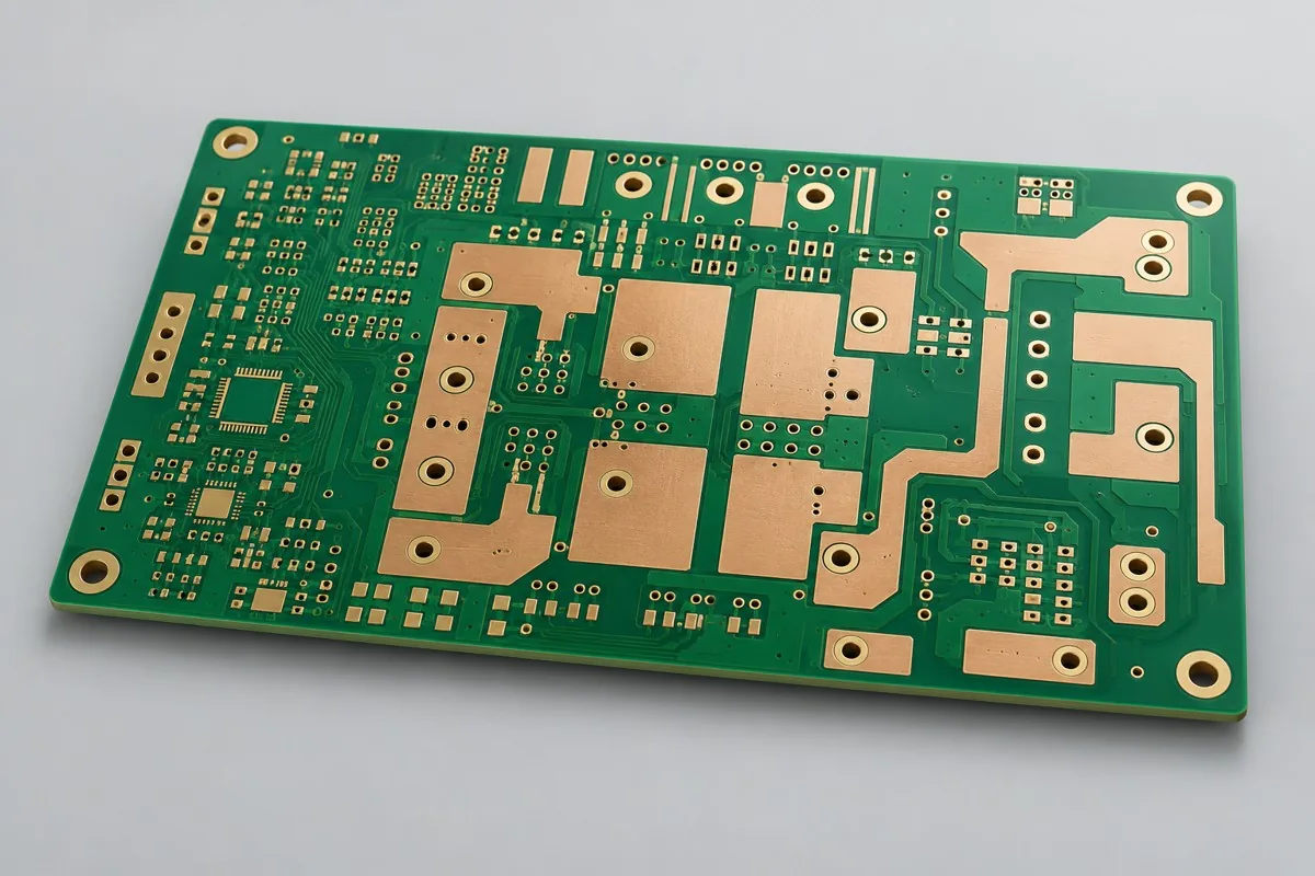
Six-layer three-ounce portable power board fabrication requires review against current fabrication drawings. This six-layer heavy-copper reference is illustrative. The inherited TG170 3/3OZ label is not a verified KFPCBA production record; procurement requires approved materials, per-layer base/finished copper, and current paths. Via arrays, narrow traces, and cooling jointly limit current. Deliver copper-weight microsections and net records; validate voltage drop and temperature rise under specified conditions.
3OZ heavy-copper PCBs first require defining bare PCB prototyping or volume-fabrication scope. Please provide Gerber data, drill files, board outline, and layer stackup, material and process requirements, quantity, and fabrication acceptance requirements. Historical six-layer TG170 3/3OZ combination; current capacity depends on copper cross section, via arrays, and cooling boundaries
Why choose this structure for three-ounce power board
A six-layer three-ounce reference can be compared when heavier supply paths and control nets share a portable power board, subject to material and process approval. State 3/3OZ explicitly; this page retains that marking without inferring the original base/finished copper definition. Added values such as the 105µm target are reference designs supporting comparison with four-layer OBC products.
How much does 3OZ heavy-copper PCB fabrication cost, and what makes up six-layer costs?
This six-layer heavy-copper product includes specified per-layer copper weight, etch compensation, resin filling adjacent to heavy-copper layers, through-hole arrays, and microsections. Historical 3/3OZ does not distinguish base and finished copper; define current targets before comparing material and copper-plating costs on repeat orders. List load-specific temperature-rise/voltage-drop tests separately; the copper-weight label does not include rated-current validation.
Quotation terms depend on the approved files, quantity, material supply, tests and delivery requirements.
Prepare a structured RFQ or use the short inquiry form.
Enter the following items in one itemized quotation: specify cost units and tax/shipping basis, with separate columns for first orders and same-revision repeat orders. The table is a procurement breakdown method, not a ready-made price list; reference specifications require approval against current fabrication drawings.
| Quotation items and pricing boundaries | Configuration inputs to confirm | Repeat orders and revision changes |
|---|---|---|
| Materials/fabrication, quoted per batch or accepted board | Historical TG170 grade unspecified; reference S1000-2M material candidate; 6-layer through-hole board; historical 3/3OZ does not distinguish base/finished copper; reference inner copper 105µm, outer base copper 70µm/finished copper 105µm | Recurs on repeat orders; material, layer-order, or copper-weight changes require requotation |
| Holes and forming, per approved hole table | Historical through holes; Ø0.40mm through-hole reference target, with power layer-transition via arrays | Repeat orders follow same-revision fabrication; check processes before changing 3OZ definitions |
| Surface finish/packaging, noting areas and batches | Reference ENIG; agree on large copper-pad thermal connections by assembly requirements | Incurred by actual batch; confirm packaging, storage conditions, and surface-finish substitutions separately |
| Engineering/tooling preparation, identifying one-time or per-batch charges | 3OZ definition: identify whether 3/3OZ means base or finished copper and which layers it applies to; provide current paths and hotspots. | Verify file revisions, ownership, and storage condition before reusing old tooling; do not assume reuse is free |
| Structural/special inspections, identifying coupons, hole groups, or samples | Approve copper-weight tables recording units and inspection locations layer by layer; historical configurations do not automatically become guaranteed values. Agree on critical trace-width/clearance and cross-sectional copper-thickness sampling in the order. | List initial prototype validation and per-batch sampling separately; quote per-board requirements separately rather than assuming everything is completed once |
| Delivery scope, reports, and accepted quantity | Bare six-layer heavy-copper PCB, historical/reference copper-definition notes, per-layer copper-weight and via-array drawings, microsections, and electrical tests; agreed thermal-validation records. | Retain revision links and batch records on repeat orders; list component assembly, firmware, and complete-unit testing separately |
Which is more cost-effective: 3OZ or 4OZ heavy-copper boards?
At equal trace width, thickness changes cross section, but 4OZ also increases fine-trace, resin-fill, and soldering thermal-capacity constraints. This page's six-layer 3OZ and four-layer 4OZ OBC products differ in application and layer count; their unit-price difference cannot establish copper-weight cost differences. Recompare copper-path width, via arrays, and assembly costs for the same circuit.
| Comparison Dimension | 3 oz heavy-copper PCB fabrication | 4 oz heavy-copper PCB fabrication |
|---|---|---|
| Material and Grade | Historical TG170 grade unlisted; S1000-2M is a reference material candidate | Historical TG150 grade unspecified; reference procurement from an approved material list meeting TG150 grade |
| Layer Count and Structure | 6 Layer Through-Hole Board | 4 Layer Through-Hole Board |
| Hole Structure and Dimensions | Historical through holes; Ø0.40mm through-hole reference target, with power layer-transition via arrays | Historical through-holes; Ø0.50mm through-hole reference target, with power-pin holes sized to components |
| Application | Automotive portable power supplies; medium/high-current DC power bare boards | OBC charger modules; bare high-current power-conversion boards |
How much current can a 3OZ copper-weight PCB carry?
Narrow traces, via barrels, connectors, and pads can all limit current. Provide continuous/peak current, path length, and permitted temperature rise; check copper cross sections and layer-transition vias first, then validate with target cooling. The 0.30mm reference minimum trace width is not a recommended high-current path width, and six layers do not mean all layers can conduct in parallel.
| Decision Sequence | Required project inputs | Agreed records and deliverables |
|---|---|---|
| 1. Define application and scope | Identify whether 3/3OZ means base or finished copper and which layers it applies to; provide current paths and hotspots. | Approve copper-weight tables recording units and inspection locations layer by layer; historical configurations do not automatically become guaranteed values. |
| 2. Confirm structural requirements | Submit narrow-trace/clearance patterns and pad dimensions to determine whether heavy-copper-region patterns need widening. | Agree on critical trace-width/clearance and cross-sectional copper-thickness sampling in the order. |
| 3. Align nets with fabrication targets | Power-net acceptance is not impedance-based; separate coupons may be defined for control differential pairs with a 100Ω reference | Provide target nets, layer pairs, and validation scope; review together with historical through-holes, Ø0.40mm through-hole reference targets, and power layer-transition via arrays |
| 4. Confirm quotation and release revision | Historical TG170 grade unspecified; reference S1000-2M material candidate; 2.00mm reference target, unspecified historically; reference ENIG, with large copper-pad thermal connections agreed by assembly requirements | Request quotations using material/pattern/inspection lists at the same revision; list unapproved substitutions as separate alternatives rather than including them in the baseline quotation |
Three-ounce power board manufacturing specifications
| Specification Items | Reference configuration or target |
|---|---|
| Illustrative structure to define | Automotive portable power supply, 6-layer through-hole board, TG170 3/3OZ |
| Material and Grade | Historical TG170 grade unlisted; S1000-2M is a reference material candidate |
| Layer Count and Structure | 6 Layer Through-Hole Board |
| Total Board Thickness | 2.00mm reference target; unspecified historically |
| Dielectric thickness and interlayer relationship | 0.20mm reference target adjacent to heavy-copper layers, balancing resin fill |
| Base Copper and Finished Copper | Historical 3/3OZ does not distinguish base/finished copper; reference inner copper 105µm, outer base copper 70µm/finished copper 105µm |
| Hole Structure and Dimensions | Historical through holes; Ø0.40mm through-hole reference target, with power layer-transition via arrays |
| Trace Width and Spacing | 0.30/0.30mm reference design; size power traces separately by voltage drop/temperature rise |
| Impedance Target and Measurement Methods | Power-net acceptance is not impedance-based; separate coupons may be defined for control differential pairs with a 100Ω reference |
| Surface Finish | Reference ENIG; agree on large copper-pad thermal connections by assembly requirements |
| Application | Automotive portable power supplies; medium/high-current DC power bare boards |
| Deliverables | Bare six-layer heavy-copper PCB, historical/reference copper-definition notes, per-layer copper-weight and via-array drawings, microsections, and electrical tests; agreed thermal-validation records. |
Trade-off between copper cross-section and via array bottlenecks
Three-ounce copper offers a larger cross section, but narrow traces, via barrels, connectors, or pads may be current bottlenecks. Six layers provide more control-routing resources, while heavy-copper etching/resin filling and soldering thermal capacity increase together. Historical application names do not establish universal rated-current guarantees.
Heavy-copper etching, edge resin fill, and thermal-relief pads: fabrication inspection
Review heavy-copper edge compensation and resin filling first; the minimum 0.30mm design does not apply to all power traces. Calculate hole-wall copper/count in layer-transition via arrays together with path length, and check large-pad thermal connections against assembly methods.
Per-layer copper-weight microsections and voltage drop/temperature rise: acceptance items
Inspect copper weight, hole-wall copper, and heavy-copper edge resin fill in first-article microsections; bare PCB net electrical testing covers power/control isolation. Measure voltage drop/temperature rise using specified loads, supply wiring, environment, and cooling conditions, then perform required interface validation on control nets.
Three-ounce power board delivery scope
Applications: automotive portable power supplies; bare medium-/high-current DC supply boards.
Bare six-layer heavy-copper PCB, historical/reference copper-definition notes, per-layer copper-weight and via-array drawings, microsections, and electrical tests; agreed thermal-validation records.
3OZ definitions, current paths, and narrow-trace clearances: RFQ inputs
Submit 3OZ definitions, current paths, and narrow-trace clearances to turn tabled design targets into inspectable fabrication drawings. The following inputs define pattern, material, or structural inspection scope; freeze the quotation revision with approved drawings.
| Project inputs required for review | Engineering decisions | Records/delivery as agreed in the order |
|---|---|---|
| 3OZ Definition | Identify whether 3/3OZ means base or finished copper and which layers it applies to; provide current paths and hotspots. | Approve copper-weight tables recording units and inspection locations layer by layer; historical configurations do not automatically become guaranteed values. |
| Heavy Copper Etching and Clearance | Submit narrow-trace/clearance patterns and pad dimensions to determine whether heavy-copper-region patterns need widening. | Agree on critical trace-width/clearance and cross-sectional copper-thickness sampling in the order. |
3OZ heavy-copper PCB fabrication: pricing, selection, and procurement FAQ
How much does 3OZ heavy-copper PCB fabrication cost, and what makes up six-layer costs?
A project-specific quotation requires review of the available files, quantity, materials, requested tests, delivery destination, taxes, shipping, and trade terms. This is not a complete finished-product quotation. Base fabrication/sample pricing, special processes, and inspections must not be billed twice. No current unit prices are published here; request an itemized quotation for the approved scope.Review quotation inputs and scope.
Which is more cost-effective: 3OZ or 4OZ heavy-copper boards?
4OZ is thicker and also increases fine-trace, resin-fill, and soldering thermal-capacity constraints; six-layer 3OZ and four-layer 4OZ additionally differ in routing resources and application. Recompare copper weight for the same circuit, layer count, and current targets rather than treating the two existing product prices as the cost of an extra 1OZ. Review the comparison
How much current can a 3OZ copper-weight PCB carry?
3OZ does not correspond to a fixed amperage; narrow traces, via barrels, contacts, and connectors can all limit current. Provide path length, continuous/peak current, and thermal conditions; check cross sections, then measure voltage drop/temperature rise. Reference minimum trace width is not a recommended high-current width. Review the comparison
Do more holes always increase a heavy-copper board's current capacity?
Hole count must be considered with finished-hole diameter, hole-wall copper, length, and connection distribution; poor layouts still create local bottlenecks. Calculate power layer-transition arrays with copper paths and verify actual hole-wall copper records.
Can a 3OZ prototype first use 1OZ to test functionality?
It can validate some low-load functions but cannot replace voltage-drop, temperature-rise, and soldering validation at target copper weight. Use final copper weight and panel structure for volume production so thin-copper prototype results are not interpreted as validation of the heavy-copper product.
Does a 3OZ board quotation include power components and heatsinks?
Bare PCB prices exclude components and cooling parts. For thermal validation under defined conditions, specify loads, wiring, environment, and installation, and list costs separately from PCB assembly and mechanical assembly to align total delivered-set prices.
How does confusing base and finished copper affect 3OZ board price comparisons?
If one quotation uses 3OZ base copper and another a 3OZ finished target, material and plating scope may differ. State units, applicable layers, and cross-section inspection locations layer by layer, then compare trace clearances, hole-wall copper, and resin-fill requirements. Historical 3/3OZ markings do not automatically mean these definitions are identical.
How can per-board and per-panel quotations for 3OZ heavy-copper PCB fabrication be converted?
Confirm 3OZ definitions and heavy-copper/signal regions layer by layer before arranging via arrays and representative cross sections; equal finished area cannot be converted using ordinary six-layer panel labor. Specify deliverable finished-board quantity per panel, actual panel purchasing quantity, and individual-board/panel delivery state. Calculate fabrication cost per board by dividing actual panel fabrication cost by the corresponding accepted finished-board quantity; list preparation, special inspection, and packaging separately. Theoretical utilization cannot promise yield.
How should first-order one-time costs and repeat-order costs be separated for 3OZ heavy-copper PCB fabrication?
For the first order, confirm documentation for 3OZ definitions, heavy-copper etching, and clearances, identifying whether related engineering, tooling, or test preparation is charged once. Approve copper-weight tables recording units and inspection locations layer by layer; historical configurations do not automatically become guaranteed values. Before reusing tooling, verify files and ownership. This batch still incurs materials, fabrication, and approved inspections; separately list preparation that must be repeated after changes rather than relying on the old order total.
Can I get a 3OZ heavy-copper PCB fabrication budget before 3OZ definition information is complete?
Start with the application, board outline, quantity, and available drawings to obtain a budget identifying missing inputs. Formal review requires identifying whether 3/3OZ means base or finished copper and which layers it applies to, plus current paths and hotspots. Corresponding deliverables require approved copper-weight tables recording units and inspection locations layer by layer, without automatically treating historical configurations as guaranteed values. Confirm fabrication/inspection quotations after these conditions are frozen. Initial inquiries need not include every file, but estimates do not imply coverage of undefined structures.
What must be reconfirmed when changing materials, hole tables, or mounting conditions on repeat orders for 3OZ heavy-copper PCB fabrication?
Submit narrow-trace/clearance patterns and pad dimensions to determine whether heavy-copper-region patterns need widening. Agree on critical trace-width/clearance and cross-sectional copper-thickness sampling in the order. Match each changed location against prior material/hole-table/mechanical files to determine whether drawings, processes, or measurements need updating. Retaining only the product name and layer count cannot establish identical repeat-order conditions.
When two 3OZ heavy-copper PCB fabrication quotations specify the same material, which configurations still need checking?
Historical 3/3OZ does not distinguish base/finished copper; align current per-layer units and cross-section locations. Compare heavy-copper clearances, resin fill, and hole-wall copper separately; the 3OZ label does not establish a universal amperage.
Which reports should link to board IDs before 3OZ heavy-copper PCB fabrication moves from prototypes to volume production?
Approve copper-weight tables recording units and inspection locations layer by layer; historical configurations do not automatically become guaranteed values. Agree on critical trace-width/clearance and cross-sectional copper-thickness sampling in the order. Link material batches, approved fabrication files, and these inspection results to current prototype IDs; use the revision with issues closed for volume production. Reports for old coupons or patterns support comparison but cannot replace current fabrication inputs. Define separate scope for complete-unit items not yet covered.
If small-batch 3OZ heavy-copper PCB unit prices fall, how can I determine whether total procurement costs really decrease?
Compare 3OZ and 4OZ on the same supply paths with identical layer resources and voltage-drop/temperature-rise targets, then account for heavy-copper etching/resin filling and assembly thermal capacity rather than using existing products with different layer counts. Total preparation, fabrication, agreed inspection, packaging, and shipping, then divide by accepted delivery quantity to compare total and per-board costs at equal scope. Use current RFQ amounts and rates rather than assuming a fixed reduction.
Comparison of three-ounce power board with adjacent board types
Current configuration distinction: historical six-layer TG170 3/3OZ combination; current capacity depends on copper cross section, via arrays, and cooling boundaries
- Four-layer TG150 four-ounce OBC charger board — Historical four-layer 4/4OZ combination emphasizes heavy-copper etching/resin filling and soldering heat; it is not a renamed six-layer board
- Six-layer partial buried copper block power control board — Local copper blocks concentrate current/heat without sacrificing signal density through whole-board heavy copper; embedded-copper processes require separate review
Heavy copper board complete product catalog · All PCB Products
Design and assembly responsibilities for three-ounce power boards
Related Functional Directions:Energy Storage BMS Sampling Control Board · Isolated power and control interface board design. These pages compare design or assembly responsibilities in the same application area. Materials, layer counts, components, and interface configurations differ; they do not share one physical model and are not extended delivery records for this engineering reference configuration.
Bare PCB validation on this page covers agreed materials, patterns, continuity/insulation, stackup, and test coupons. Design work separately covers circuits, models, and drawings; PCB assembly separately covers BOM components, soldering, firmware, and post-assembly functional tests. Before moving to related services, remap scope using final drawings/BOM; bare PCB reports cannot replace complete-unit acceptance.
Three-ounce power board material and design basis
- Engineering reference | Shengyi S1000-2M: grade, supply bases, and material documentation: grade-documentation entry point; unverified performance is not cited
- Engineering reference | PCB thermal estimates: power dissipation, copper area, and junction-temperature checks: Thermal design methods
When citing the above materials, record material revisions and design conditions for the historical six-layer TG170 3/3OZ structure; first-article review focuses on per-layer copper-weight microsections and voltage drop/temperature rise. If materials, copper weight, or via structure change, update fabrication drawings and inspection items before release.
Request Quote for This PCB Configuration: reference product ID 246, include critical circuits/interfaces and quantity, and identify specifications to retain or adjust.