
TOPIC FOCUS
Make the build-up sequence unambiguous
Layer-pair tables, via definitions, sequential-lamination notes, copper requirements, and inspection records should describe one manufacturable structure.
An HDI review should identify every microvia layer pair, build-up sequence, via-fill condition, breakout constraint, pad relationship, and the evidence required for the released design.
Layer-pair tables, via definitions, sequential-lamination notes, copper requirements, and inspection records should describe one manufacturable structure.
Microvia diameter or HDI order alone cannot establish feasibility. Material, copper, registration, aspect ratio, fill, and reliability conditions must be reviewed as a combination.
Use this topic-specific checklist with the linked engineering reference. Record the actual project conditions and the agreed acceptance scope.
| Decision | Input to confirm | Record to retain |
|---|---|---|
| Microvia structure | Layer pairs, target pads and fill intent | Via table and build-up drawing |
| Sequence | Lamination cycles, material and copper | Reviewed layer sequence |
| Verification | Registration and reliability needs | Inspection and test plan |
These records provide context for the topic. They do not replace review of the current files, materials, quantities, tests, or acceptance conditions.

Eight-layer T-BOX HDI boards: review 1-6-1 via layer pairs, package breakout, via filling, and representative microsections. All values are illustrative; approve fabrication drawings and acceptance criteria before ordering. Assembly and system verification require separate scope.
An HDI fabrication reference for relating dense interconnect structure to released board data.View Configuration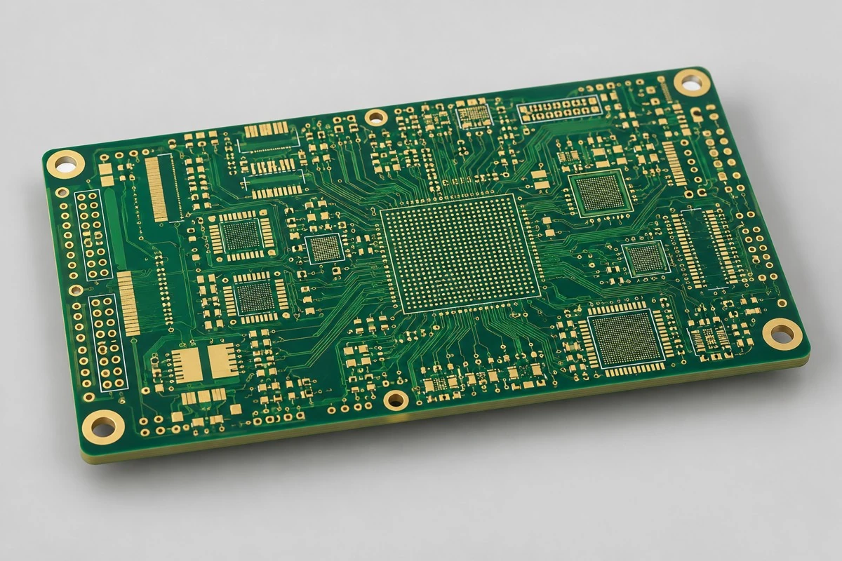
Ten-layer camera HDI boards: review 2-6-2 staggered vias, processor fanout, copper-weight options, and interconnect tests. All values are illustrative; approve fabrication drawings and acceptance criteria before ordering. Assembly and system verification require separate scope.
A compact HDI reference for checking breakout, layer-pair, and via-definition inputs.View Configuration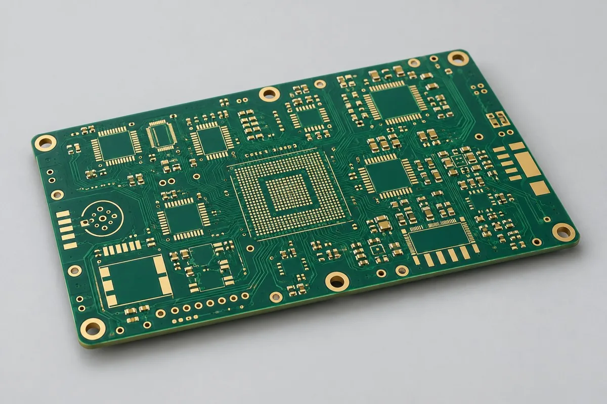
Review thin six-layer 1-4-1 HDI PCB prototyping for compact sensor modules. Define via-layer pairs, filling and pad-flatness requirements, finished copper, panel support, thickness, and warpage acceptance.
A first-order HDI prototype reference for sequential-lamination planning.View Configuration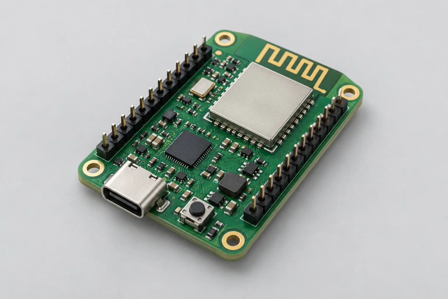
WiFi/Bluetooth core board design: for the 35mm by 30mm target, UART/SPI access, and actual enclosure, define two work packages. Module versions check antenna clearance and bridging; IC versions add crystals, matching, and RF debugging. Align prototypes, network configuration, and in-enclosure communication tests before comparing development effort and subsequent materials, rather than module/IC prices alone.
A compact wireless-board design reference where routing density can drive HDI review.View Configuration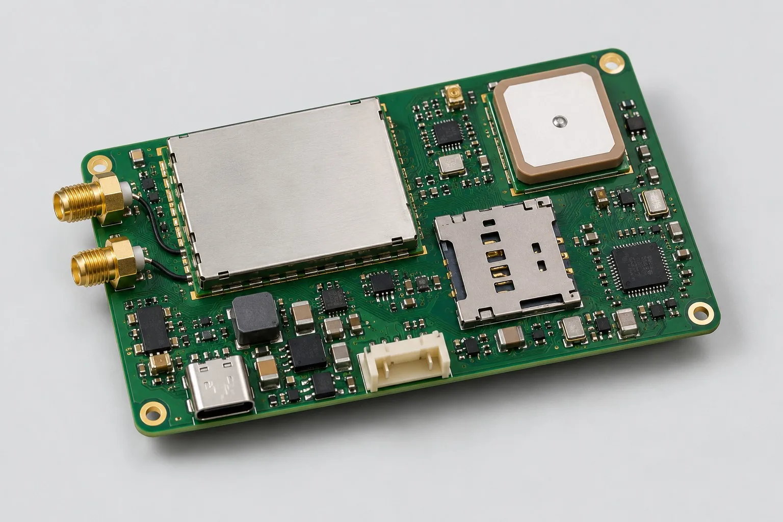
Compact 4G tracker mainboard design: freeze the 40mm by 30mm target, single-cell lithium battery/charging, battery space, and three wireless-antenna spaces before comparing six-layer through-hole and 1+4+1 HDI. Divide work into mechanical/power, location upload, buffer recovery, and complete-unit prototypes. Extremely compact routing before space is defined causes mechanical changes to consume development budgets again.
A small form-factor design reference for discussing space, escape routing, and production readiness.View ConfigurationUse this reference to check the essential inputs, then continue to the articles for specific methods and exceptions.
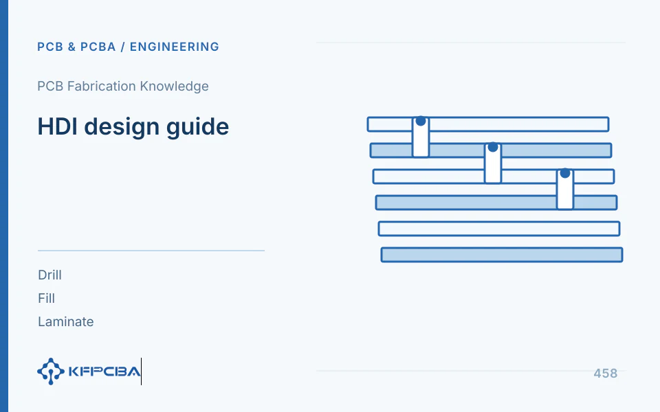
An HDI fabrication review must check each microvia group's start and end layers, depth, fill, stacked interfaces, and lamination sequence. This article uses an eight-layer via configuration and an aspect-ratio calculation to explain documentation methods, with checklists for fabrication inputs, representative cross-sections, and fault localization. It distinguishes copper-filled microvias, resin-filled vias, and tented vias.
Read Topic ReferenceFive articles are shown per page, newest first. Page 1 of 1.
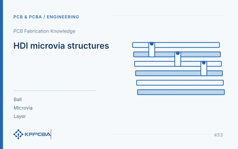
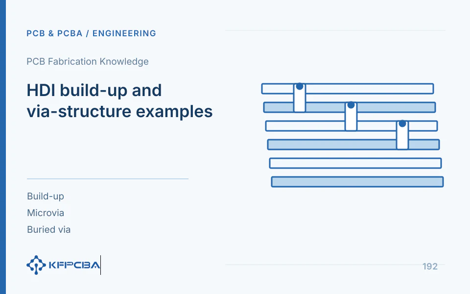
Compare related decisions. Browse all engineering topics
Share the available fabrication files, BOM, drawings, quantities, target schedule, test scope, and acceptance requirements. The response will be based on the actual project conditions.

Tell us the product use and which files are available. We can define the next engineering step even when the data package is not complete.