
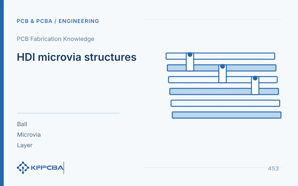
HDI microvias should solve actual breakout before layer additions/sequential lamination are selected. At equal pitch, connected balls, array size, power/ground allocation, and routing layers can require different structures. Dense BGA alone does not justify higher-order HDI, and reducing order does not justify indefinitely smaller holes/pads.
First establish connection map from pad to trace layer
Start from connected balls, distinguishing high-speed, analog, power, ground, and unconnected positions. Mark destination layers, references, and transitions. Sparse connections differ from arrays needing every inner ball escaped. Do not sacrifice reference continuity or power loops merely to fit more traces.
Divide critical areas into breakout directions, recording space used by pads, via lands, and traces. Local congestion may need local layout changes/microvias, not upgrades to all board interconnects. Show the fabricator required connections, beyond an HDI order label.
What are the trade-offs for each of the three routing escape methods
| Method | Potential Benefits | Mandatory Review |
|---|---|---|
| Through-Hole Dogbone | Intuitive routing may reduce additional layer processes | Via-land occupancy, hole aspect ratio, and inner-layer clearances |
| Micro-Via Dogbone | Short vias reduce some layer occupancy while preserving a separate pad surface | Available outer-layer channels, laser-via layer pairs, and registration |
| Microvia on Pad | Increase outer layer routing opportunities, shorten connections | Dimples, filling, copper caps, and assembly interfaces |
| Staggered or stacked microvias | Achieve more interlayer connections | Footprint, sequential lamination, and interface verification |
Würth's official HDI material shows topologies/BGA applications and supports structural comparison. Supplier dimensions/recommendations apply only under stated conditions; they do not establish another fabricator's capability.
Identify bottlenecks using available width examples
Engineering example: 0.80 mm pad pitch with 0.40 mm pad diameter leaves 0.40 mm geometric gap. One 0.10 mm trace with 0.10 mm clearance each side needs 0.30 mm and nominally fits. Two such traces with 0.10 mm between and 0.10 mm on each side need 0.50 mm, exceeding the nominal gap.
This is planar geometry only, excluding via lands, mask, tolerances, copper weight, and fabrication rules. It does not establish manufacturability but identifies channel count rather than vaguely insufficient layers as the bottleneck. Extend calculations to real balls/vias before adding routing layers or changing topology.
How via layer pairs become sequential lamination routes
Specify start/end layers, hole type, and processing cycle for every group. Outer microvias generally reach adjacent targets; deeper links require buried vias, staggering, or stacking. Equal final layer counts can have different builds, lamination, filling, and inspection effort.
- Draw final layer order with every via layer pair and reference.
- Show each lamination, drilling, and metallization cycle from inner substructures outward.
- Confirm whether later lamination/stacked vias require planar filling and copper caps.
- Map hole groups to microsection locations, electrical nets, and agreed reliability specimens.
- Approve structure after comparing manufacturing complexity, footprint, and inspectability.
Labels such as “1+N+1” summarize structures but still need actual layer diagrams and hole tables. Teams may interpret abbreviations differently; explicit layer pairs and routes govern.
How to compare higher-order versus finer line routing
| Candidate Modification | Recalculation Required | Evidence to Supplement |
|---|---|---|
| Add Signal Layers | Reference plane, total thickness, and impedance | Approve stackup and routing completion |
| Reduce trace width and spacing | Copper thickness, loss, current, and tolerances | Manufacturing combination confirmation and representative inspection |
| Change to pad-through hole | Pad-to-hole relationship and assembly window | Surface condition, solder joints, and hole connections |
| Add Microvia Layers | Via connections and build rounds | Lamination routes, interfaces, and reliability records |
No modification is inherently superior. Compare the same connection tasks and acceptance requirements; an unrouted low-cost sketch cannot be quoted directly against a completed higher-order structure.
Prototype verification must cover the genuinely difficult structures
Represent the densest breakout, critical microvia pairs, and stacked interfaces, recording actual geometry, filling, and connections. Functional power-on does not cover all via reliability; bare-board electrical testing does not establish assembly suitability of via-in-pad. Verify required environmental/thermal processes under approved tasks.
Check actual widths, dielectric thicknesses, and registration too, ensuring density was not achieved through unapproved local changes. Return manufacturing changes to sources with explicit next-revision reasons. Locate opens by via layer pair before analysis, beyond saying “HDI failed.”
Output reusable structural decision conclusions
Deliver ball connectivity, via-pair diagrams, stackup, build route, and comparisons. Explain why the structure meets connectivity, where special processes apply, and which groups verification covers. Reuse methods for later same-package projects, but recheck balls, thickness, and manufacturing conditions.
If every candidate depends on many limit exceptions, revisit component/connector placement or system partitioning. Early placement changes are generally easier to assess than repeated late hole reductions, but every change still needs electrical/mechanical review.
List unfinished connections and target layers by ball ring during breakout review. Counts track progress, not sound topology. Check references, returns, and voltage drop separately for high-speed differential, sensitive analog, and power/ground nets. After routing, review transitions/congestion so formal connectivity does not depend on excessive detours.
Cost comparisons should include coupons, filling, lamination, and assembly impacts. If one option removes a build-up cycle but adds fine-line exceptions, compare both efforts together. Document the selection basis; HDI order alone cannot rank process quality or reliability.
Preserve references and return paths during breakout
Microvias shorten connections without automatically preserving returns. After breakout to different signal layers, check changing references, suitable return connections at transitions, and required power/ground structures. Counting routed signals alone can miss these system constraints.
Include actual vias, pads, and local coupling in differential/sensitive-net models. Long detours to reduce order can alter timing/loss; complex stacked vias to shorten routes increase fabrication work. Put electrical and structural impacts in one tradeoff table.
Representative verification should include real transitions/reference changes, not only via-free straight traces. State coupon/product differences and separate supported from unsupported conclusions. After selection, give the fabricator allowable compensation and no-adjustment areas.
After package or ball-allocation changes, recheck connectivity. Existing order/via groups can start review but are not automatically still applicable. Reuse known structures and reasoning, not approvals that ignore new connections.
Frequently Asked Questions
Can equal BGA pitch reuse the same HDI order?
Also assess array size/connections, layer allocation, and thickness; pitch is only one input.
Are stacked microvias always better than staggered microvias?
It may save area, but fabrication and interface verification differ. See Microvia manufacturing verification, Manufacturing Combination with Document List.
Source material and applicable scope
- Würth Elektronik, “HDI Microvia”; current official product webpage with no fixed revision stated; checked on 2026-10-17; relevant sections: microvias, BGA density, and multilayer builds. Supports comparison by breakout/via structure. Geometry examples and selection matrices are engineering guidance; supplier capacity/dimensions are not company guarantees.
