
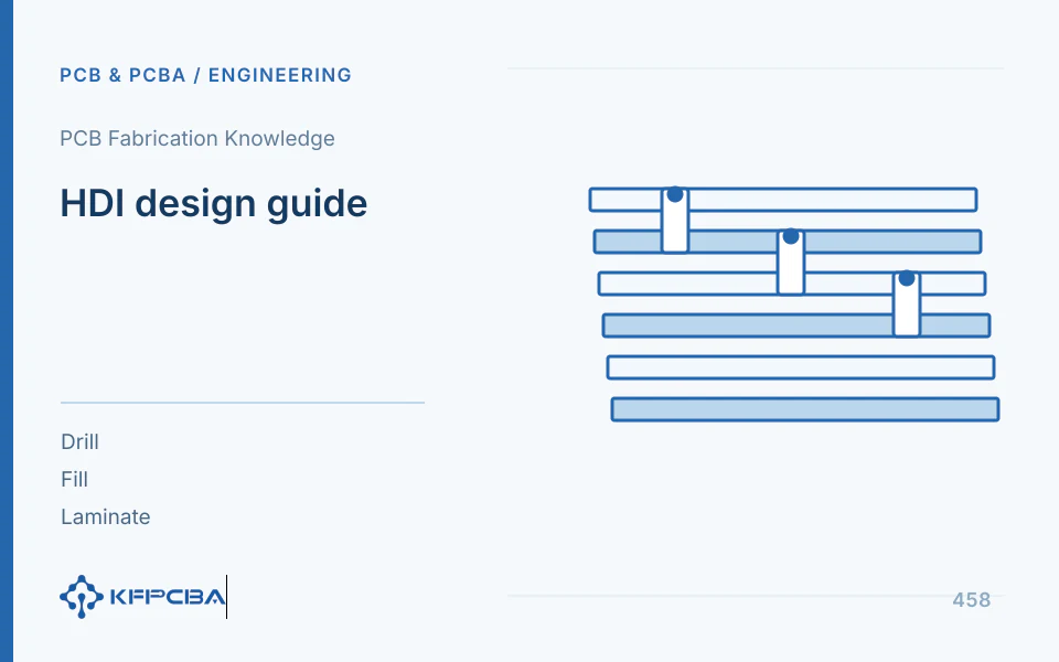
An HDI drawing that specifies only 'microvias' is incomplete. Every via group needs start and end layers, a hole-size definition, dielectric depth, fill method, and relative positioning, all matched to the lamination sequence. Staggered, stacked, and via-in-pad microvias of the same diameter may require different processes and validation. Fabrication checks should start with the specific via groups.
Establish clear identity for each hole group
The hole-group table should distinguish mechanically drilled through-holes, buried vias, and laser microvias. For each group, list layer pairs, quantities, pads, definitions for opening and bottom dimensions, target dielectric thickness, and treatment. Depth comes from the actual interlayer construction, not total board thickness. Map exported drill files to group IDs in the table so holes in CAD do not lack fabrication definitions.
| Via Group Fields | Information to provide | Function |
|---|---|---|
| Layer Pair | L1-L2 clearly defined start and end layers | Determine laser accessibility and connection objects |
| Geometry | Via opening, bottom, depth, and pad definition | Review Processing and Alignment |
| Treatment | Copper fill, resin fill, cap, or open | Determine subsequent via stacking, assembly, and surface finish |
| Relative Position | Misalignment, stacking, and connection interface | Identify local structures and inspection locations |
| Process | Lamination cycles forming via group | Correspondence with Manufacturing Route |
Terminology can follow the parties' agreement, but one generic term must not represent different physical structures.
How to express eight-layer hole group configuration
In an engineering example, an eight-layer board has L1-L2 and L8-L7 laser microvias, L2-L7 mechanically drilled buried vias, and L1-L8 through-holes. This list illustrates information presentation only; it does not establish that the construction suits every eight-layer board. Also draw the sequence for inner-layer subassemblies, buried-via formation, and outer-layer buildup, identifying which holes require filling and planarization before subsequent lamination.
- First identify the final layer sequence, distinguishing copper layers from each dielectric.
- Assign an ID to each hole group and use the same ID in plan and cross-section views.
- State whether adjacent vias are stacked, staggered, or connected only by copper traces.
- For holes requiring filling or copper capping, specify the material, surface target, and purpose.
- After the fabricator confirms the process route, recheck drill files and layer attributes in the data package.
Adding L2-L3 microvias requires more than another layer pair in the drill file; reassess the buildup and filling route. Changing via layer pairs may affect the total number of lamination cycles and the thermal exposure of existing interconnects.
Define aspect ratio calculation uniformly first
For a microvia with a dielectric depth of 0.08 mm and a review diameter of 0.10 mm, an aspect ratio defined as depth/diameter is 0.8. If another document uses diameter/depth, the same geometry gives 1.25. The ratio is reversed but the structure is identical, so state the definition in the column heading. Comparing only '0.8' and '1.25' does not establish capability.
Laser vias often have different opening and bottom geometries, so both parties must agree on the diameter used. The calculation organizes inputs; compliance with fabrication and reliability requirements also depends on materials, metallization, filling, and structural validation. A calculated ratio below a particular number does not automatically authorize release.
Select fill and copper cap based on application
Copper-filled microvias, resin-filled vias, partially plugged holes, and solder-mask-tented holes are different structures. Subsequent stacking needs a surface that supports reliable connection; via-in-pad assembly needs a planar surface; simply protecting an opening is another task. Provide a physical cross-section instead of specifying only 'via filling,' and check requirements for depressions, interfaces, surfaces, and inspection.
The Würth HDI guide discusses filling and additional processes for stacked microvias and fine-pitch designs. This supports comparing topology and fabrication together, but that supplier's dimensions cannot become guarantees for every fabricator. A separate via-filling guide can also inform hole treatment; copper-filled microvias should not automatically be classified as ordinary resin-filled holes.
How representative cross-sections cover critical interfaces
| Structure | Cross-Section Focus | Related Inspection |
|---|---|---|
| Single-Layer Micro-Via | Hole shape, bottom connection, and metal continuity | Layer pairs, conductivity, and dimensions |
| Stacked Micro-Via | Each via and interlayer connection interface | Alignment, filling, and thermal process |
| Staggered microvia | Via and connected copper area relationship | Local spacing and actual network |
| Pad Plated Hole | Filled, caps, and surface | Soldering, flatness, and assembly results |
The sectioning direction must pass through the interface of interest; cutting somewhere near a via does not establish coverage. A single cross-section has observational limits. Complete validation combines electrical testing with the reliability tests required by the project. Sample quantities and criteria must follow actual requirements, not universal void or crack limits invented from an illustrative image.
How do you locate opens, surface depressions, and registration problems?
For an open circuit, first identify the net and via layer pair, then link them to the specific lamination cycle and interface. For surface depressions, first check filling, capping, and intended use. For local registration errors, check material dimensions, datums, and alignment at each lamination cycle. Failures appearing only after assembly also require review of solder joints and thermal exposure; do not attribute every problem to laser drilling.
Retain board IDs, panel locations, raw electrical-test data, and pre-failure conditions. Corrective actions may change via construction, the route, or processing, but must identify their effects and validation targets. Enlarging a hole without examining its connection interfaces may leave the original failure unresolved.
Minimum delivery set for manufacturing approval
Deliver the final layer diagram, hole-group table, process sequence, filling notes, representative inspection locations, and documentation-package revision. Feed design and fabrication adjustments back into source files so the hole table, artwork, and production route agree. Review the effects of changes to dielectric thickness, materials, hole groups, or stacking relationships on repeat orders. Previous successful records cover only the original construction.
This article addresses how to communicate a selected construction for fabrication. If the need for additional HDI layers is still undecided, first compare the actual escape-routing requirements rather than committing to a process name before the route is clear.
How should hole-group representation connect to the inspection plan?
Start the inspection plan by listing all hole groups and their critical interfaces, then state which group each coupon or product sample covers. Holes sharing a name but differing in material, depth, fill, or lamination cycle cannot be combined solely because their diameters match. For stacked vias, show every interlayer connection interface, not just the top opening.
Sectioning direction and location affect what can be seen. An off-center cut may show a different hole shape or fill condition than a center section. State sampling and observation methods in the report and add appropriate validation when results are unclear. Visual inspection, cross-sections, and electrical tests each have their own scope; a pass in any one method must not become a conclusion about unobserved regions.
Reliability samples should undergo thermal processing representative of the product's required exposure. If a sample undergoes only one lamination while the product requires further buildup and assembly, its result cannot automatically be extended to the product. Record shared conditions and differences between sample and product, and let the test owner determine whether coverage is sufficient for the task.
When an open occurs, retain initial resistance, the affected net, and the stage at which it appeared. If the fault occurs only when hot or mechanically loaded, the test condition is itself evidence; recovery after cooling does not close the issue. Locate the connection before arranging cross-sections to avoid obtaining attractive images of unrelated vias that do not explain the failure.
Final approval should place the hole table, construction drawing, route, and inspection records under the same revision. If the fabricator proposes alternative hole groups or filling, check each associated relationship for changes. This lets recipients of repeat orders or transfers to a new fabricator understand the reason for every treatment rather than receiving only an unworkable HDI abbreviation.
Frequently asked questions
Can identical hole diameters share the same process?
Differences in depth, materials, fill, and connections still require separate confirmation.
Is bare PCB electrical test pass sufficient
Validation must also cover the reliability required by the construction and product. See HDI Routing Trade-offs, Manufacturing Combination and Document List.
Source material and applicable scope
- Würth Elektronik, HDI Design Guide; version: Version 1.2 / September 2018; checked 2026-10-17; relevant sections: microvias, BGA solutions, stacking, and HDI Microvia Standard Design Rules; scope: supports the relationships among via construction, filling, and layer sequence. Calculations and delivery tables are engineering compilations; supplier limits in an older guide are not universal standards.
