
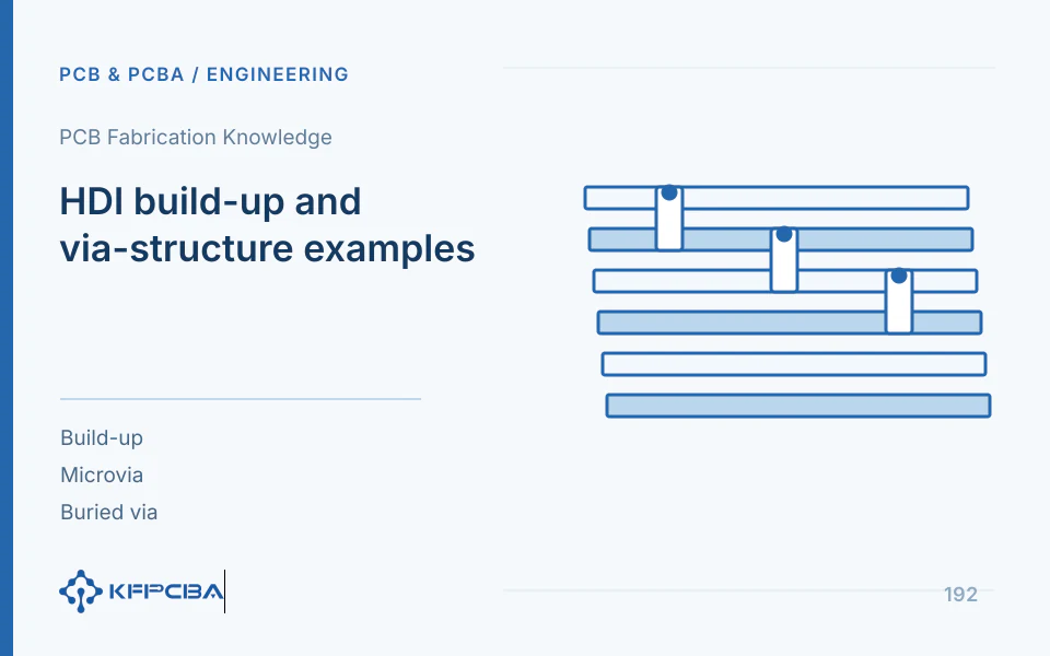
Single-stage HDI: via layer pairs and buildup stages
1+N+1 denotes one added interconnection layer on each side of the core, while 2+N+2 adds two buildup cycles. These labels do not replace complete via drawings: core buried vias, laser microvias formed in each cycle, and through holes correspond to different operations, and actual nets must be mapped individually.
| Design Issues | Content to Be Drawn | Judgment Result |
|---|---|---|
| BGA Routing Escape | Pads, tracks, and first reference plane | Is first layer microvia required |
| Connection destination layer | Start/end layers and intermediate capture pads | Can First Pass Complete Connection |
| Second buildup stage required? | Network destination after the first added layer | Is the new operation necessary |
| Staggered or stacked microvias | Hole positions, via fill, and connection sequence | Compare area and verification requirements |
One planning example
Suppose an outer-layer BGA must connect into the core: first check whether an outer-to-adjacent-layer microvia plus a core buried via completes the connection; if further connections to nets inside the buildup are needed, evaluate a second buildup cycle. This example shows only the decision path; actual components, materials, and manufacturing windows determine layer count and hole sizes.
Verify which structure needs to be covered
Each representative via chain needs a suitable test structure, with via layer pairs, materials, and lamination count recorded. Microsections check geometry and interfaces, electrical tests check continuity, and post-thermal-stress retests check stability; one continuity pass cannot replace complex-microvia reliability verification.
Inputs and outputs
Inputs: package rules, interlayer net connections, draft stackup, and via-fill requirements. Outputs: via layer-pair diagrams, reasons for stage count, process sequence, and verification structures.
HDI Routing Comparison, Hole Structure Review, HDI Layer Count vs. Structural Cost Trade-offs, Submit HDI Draft · PCB Manufacturing Knowledge
Engineering reference | HDI microvia structures: escape-routing density and sequential lamination: methodological reference; third-party design methods or material documentation do not represent KFPCBA manufacturing capabilities.
Count Total Layers and Added Layer Steps Separately
The following structures are engineering examples explaining a method, not manufacturing commitments. If the core contains 4 copper layers and each side adds 1 copper layer, the structure is 1+4+1, totaling 6 layers. If the same 4-layer core adds 2 copper layers on each side, the structure is 2+4+2, totaling 8 layers. Different total layer counts can share the same stage count, while equal total layer counts can use different core/buildup structures; six-layer or eight-layer alone is therefore insufficient for quoting.
Single-stage and two-stage are common structural abbreviations; formal documentation must still show the dielectrics, copper, and vias formed in each cycle. For asymmetric top/bottom structures, mixed via types, or any-layer connections, abbreviations are even less descriptive; check actual lamination routes. Würth's public documentation discusses microvias, buried vias, and sequential lamination separately; this article uses its structural-analysis approach without copying extreme dimensional limits.
| Structure Example | Required updated drill drawings | Cannot infer from this |
|---|---|---|
| 1+4+1 | Outer-to-adjacent-layer microvias, core holes, and through holes | Does not indicate all nets are routed |
| 2+4+2 | Specify start and end layers and connections for each added layer hole | Does not guarantee higher reliability than first-order |
| Same total layers but different core boards | Each hole pair and formation sequence | Does not indicate identical cost and route |
Describe hole chains from which network to which layer
For each representative via-chain type, identify start, end, intermediate capture pads, via positions, and filling treatment. Stacked vias save projected area but require evaluation of connection interfaces and fill condition; staggered microvias need lateral connection space and are not automatically suitable for every fanout. Do not finish routing and then ask the factory to change staggered vias to stacked vias without explanation; the change affects design and verification.
| Selection | Compare Input | Verify Output |
|---|---|---|
| Staggered microvia connection | Horizontal Space, Routing, and Capture Pads | Layer pairs, via chains, and connectivity results |
| Stacked Hole Connection | Fill, interface, lamination, and process sequence | Representative structural inspection and post-stress retesting |
| Pad Internal Hole | Surface flatness, hole treatment, and solder paste path | Manufacturing Inspection, Panel Proof, and Hidden Solder Joints |
Develop local fanout before deciding whether to add buildup stages
Method example: peripheral BGA nets escape through outer-to-adjacent-layer microvias, while inner rows remain blocked by capture pads or power references. Draw actual trace widths/spacings, pads, and interlayer connections in critical regions first, then compare changing fanout layers, core holes, component positions, or adding buildup. Two-stage construction may resolve density but also adds manufacturing and verification work; do not add operations just for reassurance without explaining the added connection task.
Nets requiring controlled impedance and continuous return paths also need adjacent reference-plane and layer-transition checks. Drawing a connected route does not establish that electrical constraints are met. After material or dielectric-thickness changes, recheck related electrical and thermal structures; do not copy trace widths directly from another manufacturer's standard stackup. After board design, communicate via-in-pad flatness and stencil risks to assembly personnel.
Deliver hole drawings along with the verification plan
- Use consistent layer names and structure identifiers, listing laser vias, mechanical holes, buried vias, and through holes by type
- Mark formation sequence, filling, and surface finish for each cycle; do not use color as the sole explanation
- Select via chains or test structures representing the most complex connections, and state inspection objectives
- Agree methods and sources of criteria for geometry, interfaces, electrical checks, and necessary post-stress retesting
- Retain actual materials, manufacturing revisions, and results, assessing retesting when via drawings change later
Passing electrical testing establishes continuity under specified conditions, not every interface's reliability; microsections observe only sampled locations. First articles should combine evidence matched to targets and identify uncovered scope. Older guide values for hole diameters or aspect ratios are not project limits; controlled design and actual manufacturing review determine current combinations.
Source material and applicable scope
- Würth Elektronik, HDI Microvia PCBs; public page does not specify a version; checked 2026-10-17; sections: High density interconnect, sequential lamination, and standard stackups. Supports microvia and buildup-structure explanations; does not transfer the company's dimensional or reliability commitments.
- Würth Elektronik, HDI Design Guide; version 1.2, 2018-09; checked 2026-10-17; sections: Through hole vias or microvias, BGA fanout, and stackup selection. Supports structural tradeoffs and manufacturing methods; historical values are not current manufacturing limits.
Why do single-stage and two-stage HDI prices differ?
Cost differences arise from actual via connections, buildup lamination, microvias, and filling work, not merely names. If single-stage construction completes package fanout and interlayer connections, extra buildup may add no application value; if space and connections cannot be achieved, forcing fewer stages may require different components or a larger board outline.
Compare costs and verification under the same conditions
Compare component pitch, board outline, every via layer pair, and reference planes in one drawing. Inquiries should cite the complete stackup and via drawing and list representative via-chain inspections; total layer count is not a substitute for stage count or reliability.
View services and configurations related to this question or Request a project quotation. For initial discussions, describe the intended use, available documentation, and expected quantity.
Related procurement and acceptance Q&A
Why do single-stage and two-stage HDI prices differ?
See: Why do single-stage and two-stage HDI prices differ?
Is a six-layer HDI always second-order?
Total layer count does not equal buildup stage count. Examine the core, each buildup cycle, and microvia start/end layers, then describe the structure with a complete via layer-pair diagram.
See: Single-stage HDI: via layer pairs and buildup stages
If single-stage HDI supports escape routing, is upgrading to two-stage worthwhile for reassurance?
First verify whether actual nets require added buildup connections; if single-stage construction already meets needs, extra operations may add no application value. Keep board-outline and package constraints consistent in comparisons.
Why do HDI quotations require filling and stacked-via requirements?
Via positions, filling, and connection sequence affect routes and verification; stage names alone are insufficient. Provide via layer-pair drawings and representative via-chain requirements so manufacturers can define process scope.
Can via-chain reliability verification be omitted after HDI electrical testing passes?
One continuity test cannot replace complex-microvia stability verification. Link representative via chains to materials, lamination count, and inspection methods, and accept against agreed thermal-stress and retesting scope.
