
TOPIC FOCUS
Connect electrical targets to the physical stackup
Identify single-ended or differential nets, reference planes, trace geometry, copper stage, material data, compensation authority, coupon location, and TDR reporting.
Controlled-impedance release requires target values and tolerances tied to named nets, actual reference layers, stackup geometry, dielectric data, coupon design, and an agreed measurement method.
Identify single-ended or differential nets, reference planes, trace geometry, copper stage, material data, compensation authority, coupon location, and TDR reporting.
A nominal impedance value does not define the construction. Final geometry and acceptance depend on the released stackup, selected material data, manufacturing compensation, and measurement agreement.
Use this topic-specific checklist with the linked engineering reference. Record the actual project conditions and the agreed acceptance scope.
| Decision | Input to confirm | Record to retain |
|---|---|---|
| Electrical target | Named nets, topology, target and tolerance | Net-to-impedance table |
| Physical build | Reference planes, dielectric and copper state | Approved stackup and trace geometry |
| Measurement | Coupon location and TDR method | Report identifier linked to nets |
These records provide context for the topic. They do not replace review of the current files, materials, quantities, tests, or acceptance conditions.
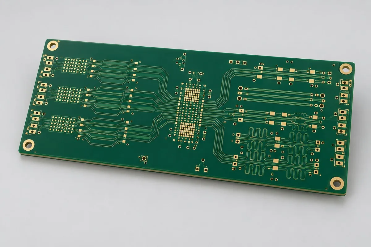
Six-layer impedance prototypes: review target nets, representative coupons, measured stackups, and raw TDR records. All values are illustrative; approve fabrication drawings and acceptance criteria before ordering. Assembly and system verification require separate scope.
An impedance-board prototype reference for connecting target nets, stackup, and test evidence.View Configuration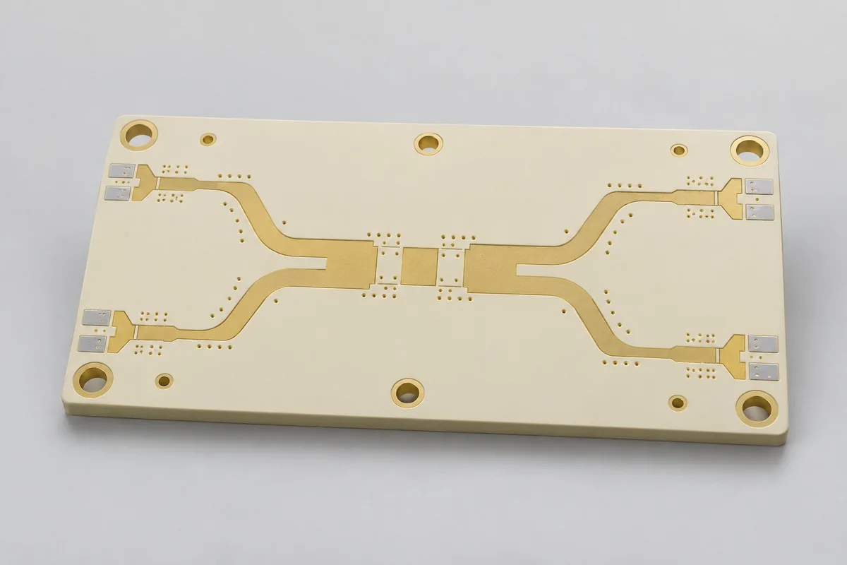
RO4350B high-frequency PCB fabrication reviews materials, structures, and delivery scope against connectors, ports, and exposed-copper RF regions. It provides cost breakdowns, one-time preparation and same-revision repeat-order boundaries, configuration-selection steps, and quotation conversion methods. Specifications follow approved fabrication drawings; component assembly and complete-unit validation are agreed separately.
A high-frequency laminate reference where dielectric data and geometry must be identified together.View Configuration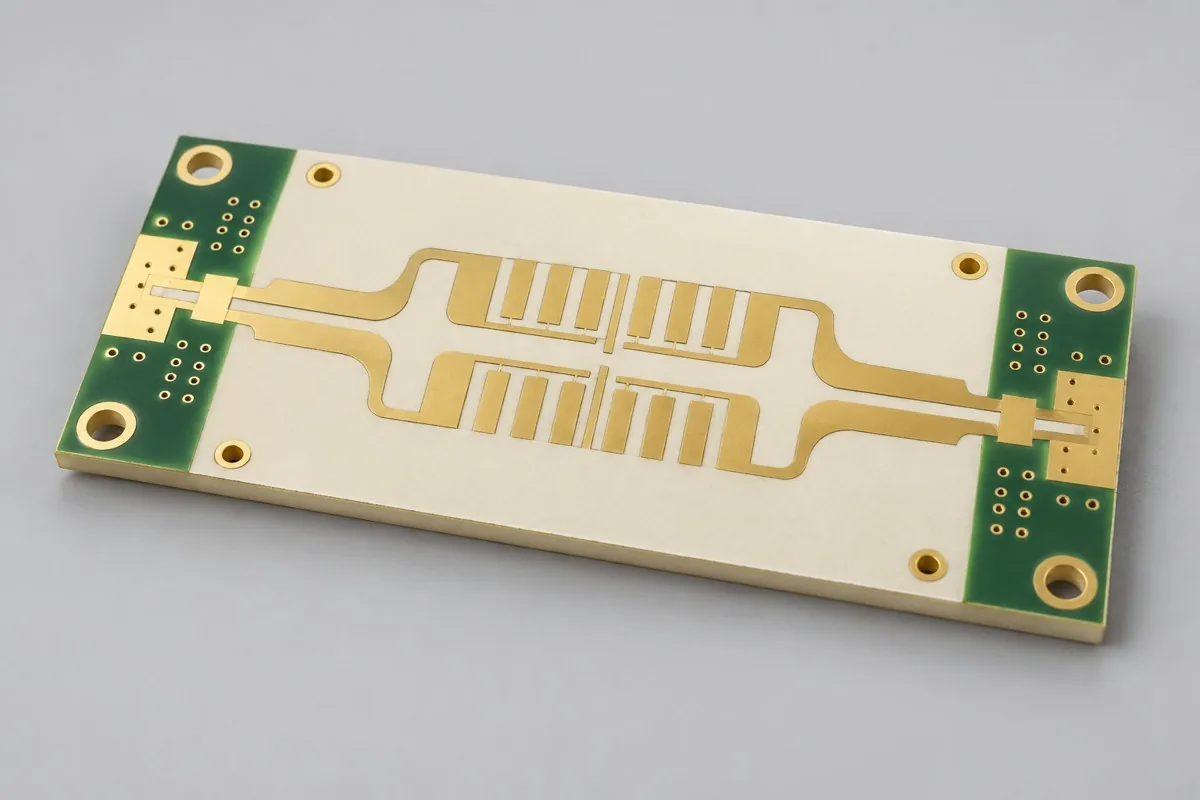
RO4003C high-frequency PCB prototyping reviews materials, structures, and deliverables against resonant/coupled artwork and material/frequency deviations, with cost breakdowns, one-time setup and same-revision reorder boundaries, configuration selection steps, and quotation conversion methods. Specifications follow approved fabrication drawings; component assembly and complete-system verification are separate.
A high-frequency prototype reference for discussing material identity and controlled structures.View Configuration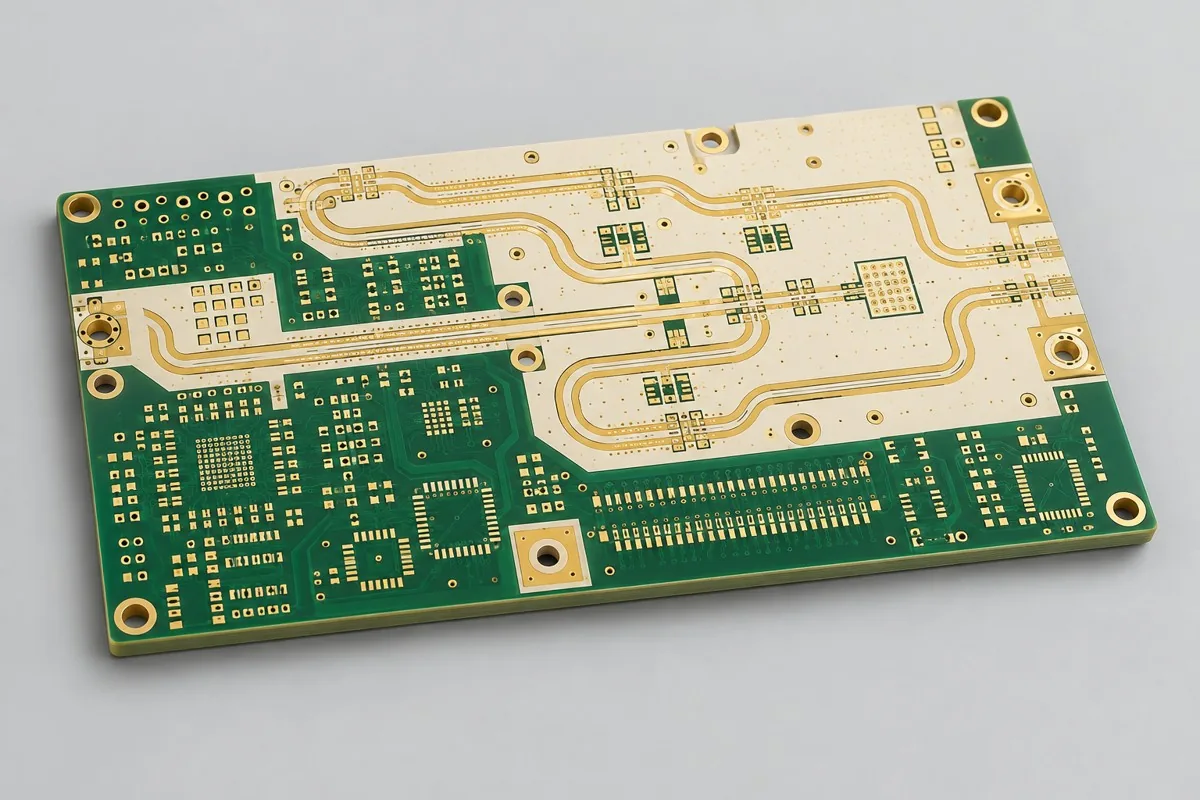
Review a six-layer RO4350B/FR4 hybrid PCB with one RF surface and digital control layers. Define RF reference planes, interface returns, lamination requirements, and separate RF and digital acceptance.
A hybrid-material reference where different dielectric systems affect stackup review.View Configuration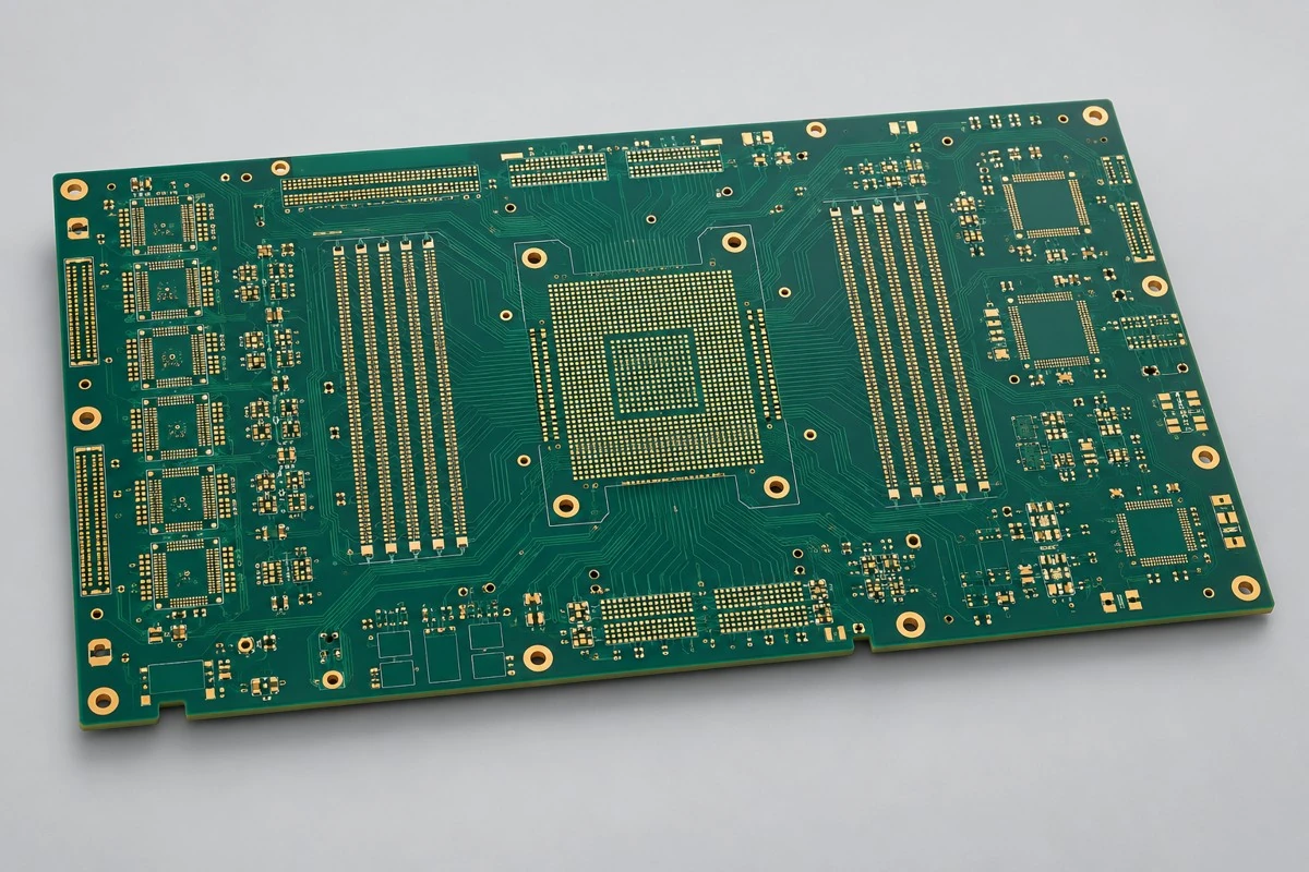
Review a twelve-layer low-loss PCB with backdrilled high-speed vias. Define entry sides, retained layers, protected copper, and measurable residual-stub targets alongside impedance and link-verification scope.
A multilayer high-speed reference for linking signal layers, reference planes, and verification.View ConfigurationUse this reference to check the essential inputs, then continue to the articles for specific methods and exceptions.
Controlled-impedance PCB purchasing must map target nets, actual layer pairs, manufacturing geometry, and test coupons to one another. This article adds a TDR definition, a reflection-coefficient example, calibration and measurement-window tables, and an abnormal-result retest process. It explains single-ended and differential measurement boundaries so one passing coupon report is not substituted for complete interface verification.
Read Topic ReferenceFive articles are shown per page, newest first. Page 1 of 1.
Compare related decisions. Browse all engineering topics
Share the available fabrication files, BOM, drawings, quantities, target schedule, test scope, and acceptance requirements. The response will be based on the actual project conditions.

Tell us the product use and which files are available. We can define the next engineering step even when the data package is not complete.