
TOPIC FOCUS
Give the prototype a specific learning objective
Separate fit, electrical function, process learning, firmware, test development, regulatory work, and pilot preparation so the build quantity and evidence match the decision.
Prototype planning starts by defining what the build must prove, then aligning fabrication files, BOM and placement data, quantity, acceptance criteria, test evidence, and the decision required before the next build.
Separate fit, electrical function, process learning, firmware, test development, regulatory work, and pilot preparation so the build quantity and evidence match the decision.
A successful prototype does not automatically prove volume readiness. Material availability, fixtures, programming, inspection, yield controls, traceability, process windows, and change control need separate release evidence.
Use this topic-specific checklist with the linked engineering reference. Record the actual project conditions and the agreed acceptance scope.
| Decision | Input to confirm | Record to retain |
|---|---|---|
| Learning goal | Fit, electrical, process or firmware question | Decision the prototype must answer |
| Build inputs | Files, BOM, quantity and test conditions | Versioned build and acceptance package |
| Next build | Failures, changes and unresolved risks | Retest and pilot-readiness record |
These records provide context for the topic. They do not replace review of the current files, materials, quantities, tests, or acceptance conditions.
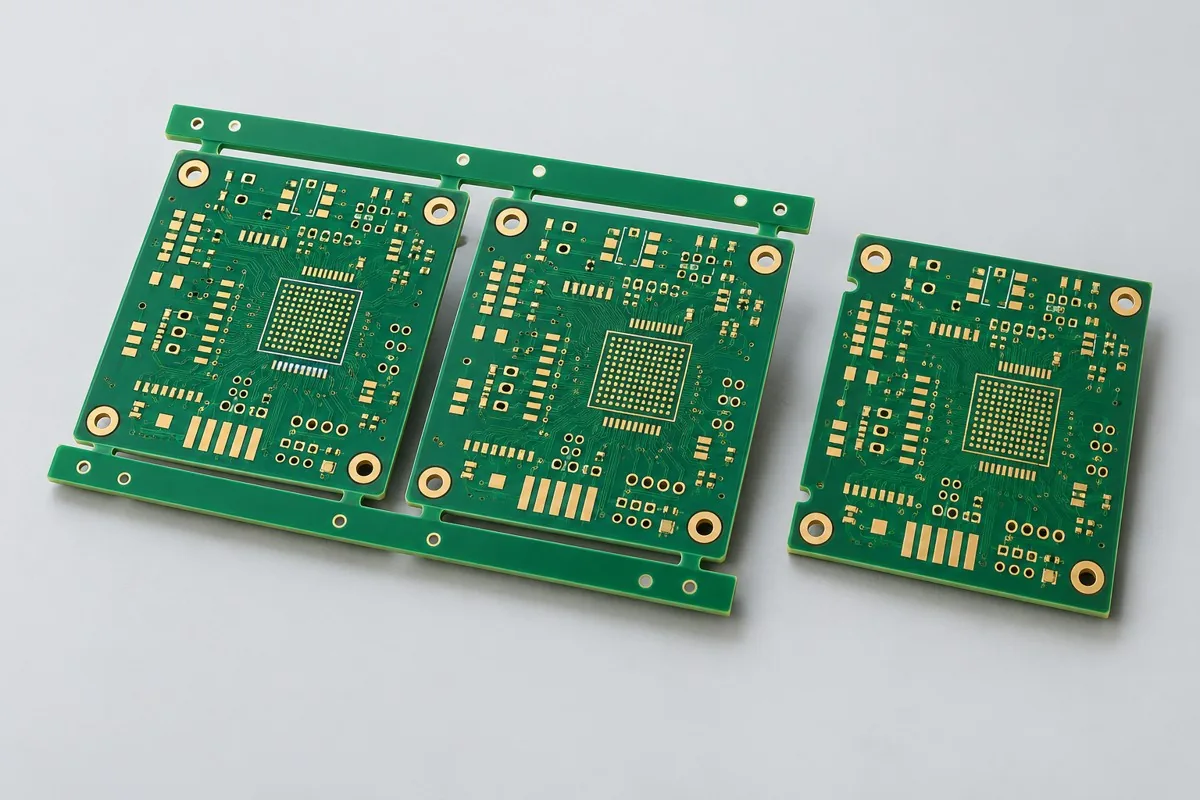
Four-layer functional prototypes: review verification objectives, Gerber revisions, sample variants, and production change records. All values are illustrative; approve fabrication drawings and acceptance criteria before ordering. Assembly and system verification require separate scope.
A four-layer prototype reference for establishing fabrication inputs and build intent.View Configuration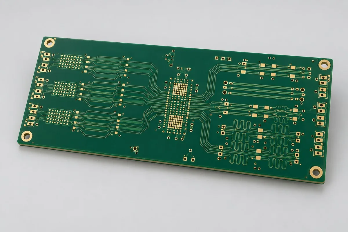
Six-layer impedance prototypes: review target nets, representative coupons, measured stackups, and raw TDR records. All values are illustrative; approve fabrication drawings and acceptance criteria before ordering. Assembly and system verification require separate scope.
An impedance prototype reference for connecting learning goals to test evidence.View Configuration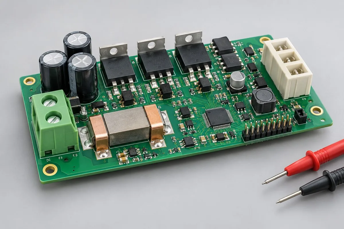
Motor driver prototype assembly references cover three-phase drives and current/position-feedback checks. Compare materials, SMT, later-installed power parts, staged power-up and energy-limited testing. Define gate, phase-sequence, sampling, controlled-load and protection tests, and retain measurement records and component-change revisions.
A motor-driver prototype reference for assembly, thermal, and functional review.View Configuration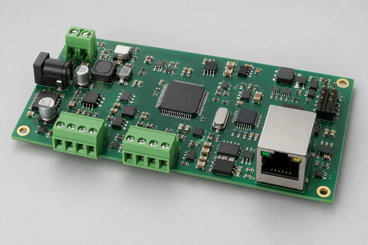
Communication interface prototype PCB assembly reference configurations cover serial/bus/network interface verification. Separate SMT, interface post-soldering, test software, and protocol integration testing; compare material supply, setup, and per-lot assembly costs. Check loops, packets, error injection, and power-loss/disconnection recovery scope, plus samples + packets/waveforms + issue/revision-list deliverables.
A communication-interface prototype reference for defining test and acceptance needs.View Configuration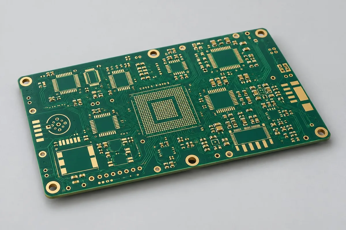
Review thin six-layer 1-4-1 HDI PCB prototyping for compact sensor modules. Define via-layer pairs, filling and pad-flatness requirements, finished copper, panel support, thickness, and warpage acceptance.
An HDI prototype reference for planning a constrained fabrication learning cycle.View ConfigurationUse this reference to check the essential inputs, then continue to the articles for specific methods and exceptions.
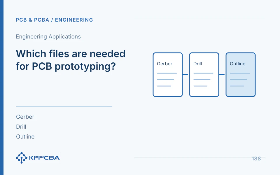
Prepare a consistent PCB fabrication package with Gerber data, drill files, board outlines, a revision manifest, stackups, and via layer pairs. Resolve conflicts between drawings, drill dimensions, and fabrication notes before release.
Read Topic ReferenceFive articles are shown per page, newest first. Page 1 of 1.
Compare related decisions. Browse all engineering topics
Share the available fabrication files, BOM, drawings, quantities, target schedule, test scope, and acceptance requirements. The response will be based on the actual project conditions.

Tell us the product use and which files are available. We can define the next engineering step even when the data package is not complete.