
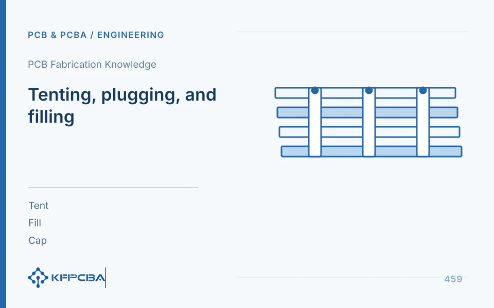
Tenting covers a hole opening, plugging places material partly inside the hole, filling targets complete fill, and copper capping creates a copper cover over a filled hole. These are not different names for one process. If a component will be soldered over a via, confirm the solderable plane and connection structure. Specifying only 'plugging' does not define a via-in-pad construction.
Select structure first using functional goals
Preventing solder entry, avoiding trapped media in holes, protecting annular rings, maintaining a vacuum during testing, obtaining a planar surface, and improving heat transfer require different structures. A location may have two simultaneous objectives; specify both. Whether the via lies within a component pad, contacts a heat sink, or undergoes later lamination changes the selection.
| Target | Structures That Need Clarification | Cannot be directly inferred |
|---|---|---|
| Hole Wall Protection | Covered side, covering material, and hole condition | Via Fully Filled Inside |
| Prevent Dielectric from Entering Via | Closed scope and continuity requirements | Permanent sealing in any environment |
| Assembly on Pad | Fill, copper caps, and surface flatness | Standard solder mask via opening can form solderable plane |
| Subsequent Lamination | Via cavity fill and planarization | Appearance Coverage Is Sufficient |
Define the function first so the fabricator can choose an executable process. Specifying only a process name without its purpose may produce something that formally matches the request but cannot be assembled.
How can IPC types be used without extending their meaning?
Würth's Plugging–Filling–Tenting, Version 1, December 2019, uses public illustrations to distinguish III-a single-sided partial plugging, V complete filling, VI-a/VI-b filling with single-sided or double-sided solder mask coverage, and VII filling with copper capping. This discussion follows that guide's explanation; it does not claim to have read or replace the full IPC-4761 standard.
The guide also presents copper-filled microvias separately and states that they are not classified under the same ordinary-hole treatment descriptions. Orders should provide both an actual cross-section and text so a type number alone does not omit hole type, filler, or surface requirements. The supplier's statement in that version that it does not offer plain tenting also does not establish whether other fabricators offer it.
Why are hole cavity volume examples useful?
For an ideal cylinder, a hole 0.30 mm in diameter and 1.60 mm deep has a cavity volume of V=πd²h/4≈0.113 mm³. Increasing the diameter to 0.60 mm at the same depth gives approximately 0.452 mm³, four times the volume. This example shows only that fill volume scales with the square of diameter; it is not a method for calculating filler formulations, allowable voids, or solder loss.
Real holes have hole-wall copper and shape variation, and blind vias and through-holes use different filling methods. Solder uptake by an untreated hole under a pad also depends on wetting, paste printing, reflow, and surface conditions. The entire hole volume cannot directly predict the solder joint. Use the calculation to identify sensitive dimensions, then validate with assembly samples.
How to write per-group via processing table
| Field | Example expression format | Consistency with where |
|---|---|---|
| Hole Group | V1, L1-L8 mechanical plated holes | Drilling Files and Layer Map |
| Application | Under component heat dissipation pad, need solderable plane | Package and assembly drawing |
| Fill and Cover | Clearly define fill, copper cap, and two-sided status | Process confirmation and cross-section drawing |
| Surface Requirements | Depressions, protrusions, and inspection basis listed separately | Manufacturing drawing and acceptance plan |
| Inspection | Appearance, cross-section, and assembly results | Representative Location and Board Number |
The example does not assume every hole needs the same treatment. Group non-pad vias, buried vias, and heat-sink contact regions by purpose. If only some holes require filling and capping, provide an identifiable scope in the data rather than making the factory infer requirements from each pad location.
Via processing reviewed together with stencil and solder mask
The surface after filling affects solder-paste deposition and component support. Vias in thermal pads also interact with stencil windowing, solder volume, and voiding. Ordinary solder mask coverage does not provide the same function as thermal contact and may be unsuitable as a load-bearing surface. Design, PCB fabrication, and assembly teams should agree on the same cross-section before the first article.
For open-hole structures, assess solder loss, backside solder balls, and related risks. For capped structures, check copper-surface integrity, planarity, and solderable finish. Do not temporarily change hole treatment on the shop floor to solve an assembly issue unless design and manufacturing effects have been reviewed and approved.
What can be seen separately in appearance and cross-section
- Visually inspect opening coverage, copper surfaces, contamination, and obvious depressions or protrusions, linking observations to board IDs and locations.
- Use cross-sections to inspect internal fill, interfaces, and capping, stating the sampling direction and represented hole group.
- Use electrical testing to check the intended connections; filler appearance alone does not establish continuity.
- Inspect assembly samples for solder loss, joint condition, and component condition against product criteria.
- Add environmental or thermal-process validation when required by the actual application; do not invent a universal void percentage.
Visual inspection cannot reveal the entire hole cavity. An attractive opening does not prove a defect-free interior, and a single cross-section also has observational limits. The inspection plan should make different methods complementary rather than assigning all release decisions to one image.
How to check solder wicking, solder balls, and lifting?
If solder enters a hole, check whether actual hole treatment matches the drawing and whether the cap is intact, then examine paste printing and reflow. For backside solder balls, check whether the hole is open through the board, the backside mask opening, and solder paths. For floating components, check solder volume, surface protrusions, and gas escape. These different symptoms cannot all be resolved by 'changing to plugging.'
For local depressions after filling, first confirm the measurement location and functional requirements, then examine filling and capping. If a problem appears only after assembly, retain pre-assembly surface evidence. Link original photographs, cross-sections, electrical tests, and soldering records to the same lot to distinguish incoming construction from assembly effects.
How can change control prevent identical names from concealing different structures?
Record the approved construction in the hole table and schematic cross-section, with procurement and engineering clarifications referencing the same revision. If the fabricator proposes a different filler, covered side, or cap, recheck soldering, insulation, and thermal requirements. Repeat orders must verify the specific process and surface condition, not just the word 'plugging.'
For thermal applications, resin fill, hole-wall copper, and copper fill create different heat paths. Analyze the actual materials and contacts rather than equating 'filled vias' with high thermal conductivity. For insulation, arbitrary solder mask coverage also does not establish the insulation evidence required for the product.
How can drawing requirements align with factory hole-treatment terminology?
Different teams may informally call partial filling, complete filling, and surface coverage 'plugging.' During confirmation, use a cross-section to identify the material inside the hole, the material at the opening, and the solderable side. Once the actual construction is clear, use the supplier's process name as a supplementary field to prevent identical names from representing different structures.
If the drawing and quotation use different terms for a hole group, first determine whether this is only terminology or an actual change in filler, covered side, or cap. A terminology difference can be resolved with a cross-reference record; a physical change requires an engineering impact assessment. Do not merely standardize wording without checking the cross-section, and do not automatically reject a construction because its name differs.
Approve the acceptance plan with the construction. Via-in-pad structures emphasize a solderable plane; other holes may emphasize protection or subsequent lamination, so inspection targets differ. If numerical requirements are undefined, identify the measurements and criteria sources needing confirmation instead of adding an unagreed limit after production based on personal experience.
Record surface, hole-interior, and assembly results separately so a good result in one area does not conceal a gap in another. After construction approval, changes to mask openings or assembly processes still require checking whether the original treatment remains appropriate, especially when a previously unsoldered via becomes an assembly pad.
Frequently asked questions
Does covering a via with solder mask make it suitable for via-in-pad?
If a solderable plane is required, confirm filling and copper capping. Ordinary tenting does not automatically meet that requirement.
Do all thermal vias require copper caps?
The location and assembly objectives determine the choice. For more information, see Thermal Via Interface, Manufacturing Combination with Delivery List.
Source material and applicable scope
- Würth Elektronik, Design Guide Plugging–Filling–Tenting; version: Version 1 / December 2019; checked 2026-10-17; relevant sections: construction definitions, types, and application table on pages 2 to 4; scope: supports distinctions among plugging, filling, tenting, and copper capping and the types listed in the guide. It does not replace the full IPC-4761 standard. The volume calculation and inspection methods are engineering compilations.
