Company Address
201, Factory 6, Longhui Industrial Park, Fuqiao 3rd District, Xinhe Community, Fuhai Street, Baoan District, Shenzhen, Guangdong, China

NEWS & ENGINEERING

PCB Fabrication Knowledge

Explore PCB fabrication guides on materials, stackups, vias and prototype planning. Connect design files with manufacturing and acceptance requirements.

Engineering Resources

PCB · PCB ASSEMBLY · DESIGN · PROCUREMENT AND ACCEPTANCE

PCB Fabrication Knowledge

What should controlled-impedance PCB prototypes confirm? Nets, stackups, and test coupons

Controlled-impedance PCB purchasing must map target nets, actual layer pairs, manufacturing geometry, and test coupons to one another. This article adds a TDR definition, a reflection-coefficient example, calibration and measurement-window tables, and an abnormal-result retest process. It explains single-ended and differential measurement boundaries so one passing coupon report is not substituted for complete interface verification.

Read Article
PCB Fabrication Knowledge

Two-, four-, or six-layer PCB prototypes? Compare by verification task

PCB layer count should follow component escape routing, continuous reference planes, power requirements, and verification tasks. Beyond comparing two, four, and six layers, this article adds a layer-reduction decision table and a two-option review process. It explains which nets, vias, and tests change with layer count, helping compare total redesign cost rather than bare-board unit price alone.

Read Article
PCB Fabrication Knowledge

Should PCBs be ordered as individual boards or panels? Quantities, delivery, and pricing basis

PCB panel orders should distinguish accepted individual boards, delivered assembly panels, and fabrication panels. Beyond quantity definitions, this article adds defective-position counts, a panel-area example, and a responsibility table. It specifies process rails, coupons, marks, depaneling, and allowances so quotations, assembly, and acceptance share one delivery basis.

Read Article
PCB Fabrication Knowledge

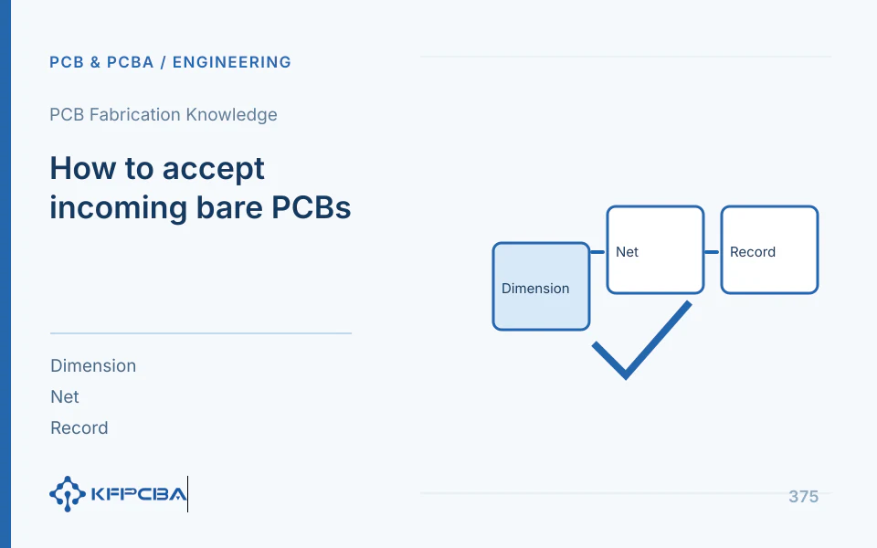
How to accept incoming bare PCBs: dimensions, electrical testing, and issue records

Bare PCB acceptance should link approved drawings, board identification, lots, quantities, and measurements. Beyond the incoming checklist, this article adds a dimensional decision example, staged inspection, and evidence tables. It distinguishes electrical testing, TDR coupons, materials, and functional results, and outlines retesting, quarantine, and deviation acceptance so issues can be reproduced and closed.

Read Article
PCB Fabrication Knowledge

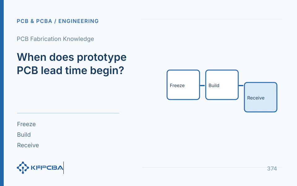
When does prototype PCB lead time begin? Engineering approval and arrival milestones

PCB lead time should distinguish file receipt, engineering approval, materials, fabrication, shipping, and acceptance. Alongside a milestone checklist, this article adds parallel tasks, a backward-scheduling example, an expedited-order responsibility table, and revision-hold records, showing how a requested arrival date becomes a confirmable schedule. Dispatch dates and logistics estimates must not be treated as commitments for accepted-board arrival.

Read Article
PCB Fabrication Knowledge

How to compare prototype PCB quotations: files, costs, and quantity definitions

Before comparing prototype PCB quotations, align the manufacturing revision, accepted quantity, materials/processes, inspection, and tax/shipping inclusions, then compare total costs. This article retains the public budgeting framework and adds a hypothetical quotation normalization example and process response table to identify setup fees, panel quantities, and exclusions, preventing a low unit price for a different configuration from being mistaken for lower procurement cost.

Read Article
PCB Fabrication Knowledge

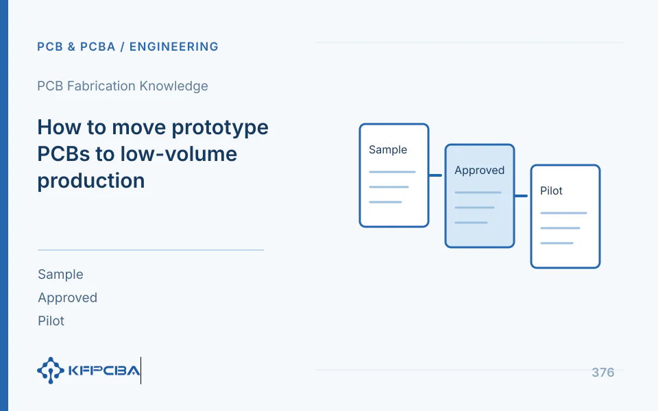
How should materials be prepared for small-batch PCB prototypes? Laminate substitution and productio

Extends small-batch PCB material preparation and production-transition guidance with consistent material-substitution comparisons, separate verification objectives, and approval records. Distinguishes database typical values from specific grade parameters, calculates cutting quantities and cost boundaries, and supports complete transfer of actual sample configurations to later production.

Read Article

PCB fabrication resources: understanding fabrication through structures and materials

HDI structure and low-volume material preparation involve two separate decisions: define via layer pairs and build-up layers, then assess how material availability and substitutions affect validation.

PCB / PCBA · PROJECT ENQUIRY

Does Your Project Need PCB Fabrication, Assembly, or Box Build?

Tell us the product use and which files are available. We can define the next engineering step even when the data package is not complete.

Call UsWhatsAppRequest a Quote