
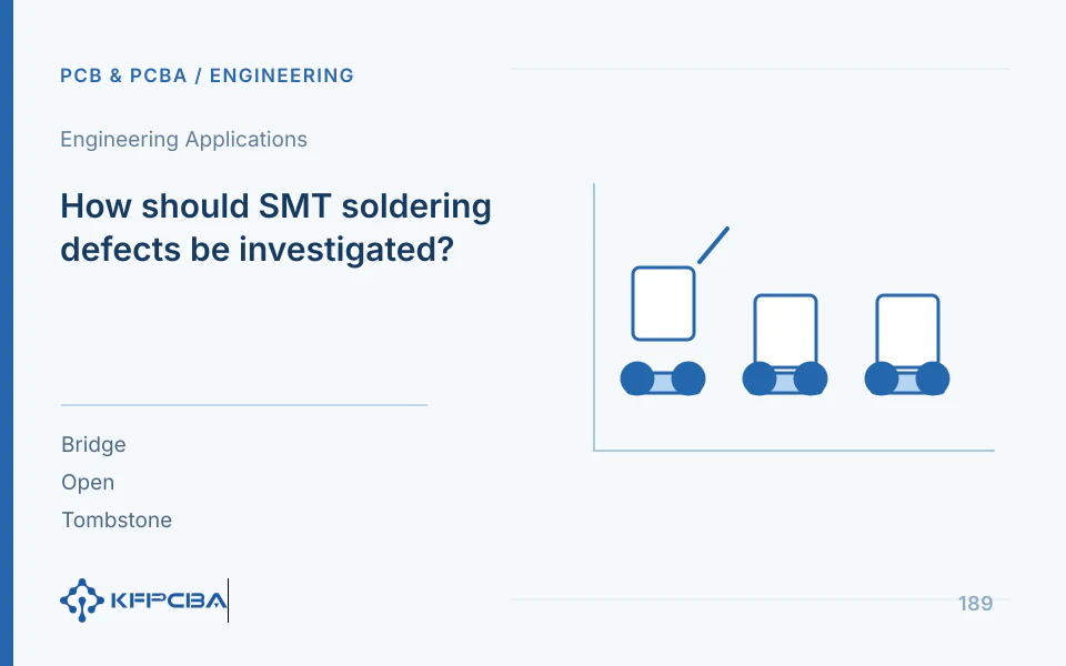
SMT soldering defects: collect evidence before adjusting the process
Tombstoning, bridging, insufficient solder, and voids can have multiple causes. Identify affected reference designators, lots, and locations before comparing printing, component, board, and thermal-process records. A single symptom does not establish one fixed remedy; separate acceptance from fault diagnosis.
Phenomena, Candidate Causes, and Verification Directions
| Phenomenon | Potentially relevant factors | Evidence to collect first | Verification Trade-offs |
|---|---|---|---|
| Tombstoning | End-to-end wetting/thermal response, pad and printing imbalance, and component condition | Solder paste and pads at both ends of the component, hot/cold locations, profiles, and material lots | Change one factor and compare both ends; do not assume every tombstone results from fast heating |
| Bridging/Solder Bridges | Solder-paste volume, apertures, print or placement offset, and component spacing | Print images, offset direction, stencil, and component lead condition | A thinner stencil may cause insufficient solder on other components, requiring joint evaluation |
| Insufficient Solder/Open Circuit | Insufficient paste release, solder wicking into holes, solderability, placement, and thermal processes | Solder-paste volume/shape, via treatment, original manufacturer materials, and measured profiles | Adding solder does not necessarily resolve solderability or uneven heating |
| Void | Pad structure, solder volume, flux volatilization, and reflow | Current solder paste, holes/apertures, temperature measurements, and suitable hidden-joint inspection | Evaluate against package use and agreed acceptance criteria; do not apply one void-percentage limit universally |
| Misalignment | Positioning coordinates, print offset, support, pick-and-place, or reflow changes | First-article orientation, fiducial, coordinates for both sides, and states at each operation | Distinguish problems arising before versus after reflow, then adjust the relevant operation |
Why a thinner stencil is not an automatic response to solder bridging
The same board may contain fine-pitch ICs and large thermal pads. Reducing overall stencil thickness may improve IC bridging but leave large pads short of solder. Compare local apertures, support, and paste release first, then evaluate local design changes or other options; after changes, inspect the whole board rather than only the original defective reference designators.
Validate reflow using current solder-paste and component conditions
Kester's solder-paste guidance states that processes vary with board thickness, components, and equipment. Recommended profiles provide a starting point; production still requires temperature measurements at solder joints or representative locations, checking current solder paste, component limits, and cumulative oven passes. Oven-zone setpoints are not solder-joint temperatures.
Example record of one-time troubleshooting
If resistor tombstones in a batch cluster near board edges, retain defect locations and initial conditions first, then compare paste printing at both ends, pads and thermal connections, edge support, and temperature measurements. Trial one evidence-backed factor, retain a control batch, and recheck other packages. Record before/after conditions, quantities, and acceptance judgments; this example demonstrates a method, not an actual KFPCBA production case.
Customer input and engineering output
Prepare board/BOM/stencil revisions, photos of defective reference designators, lots and quantities, original process/temperature records, and component/PCB condition. Engineering outputs should include candidate causes, missing evidence, single-variable verification, results, and release recommendations. Confirm actual inspection tools and equipment; references here to SPI/AOI or X-ray inspection do not establish factory equipment availability.
Next Steps Confirmed by Question
SMT Service: Convert troubleshooting methods to pilot production reviews.
Factory Inspection: distinguish inspection coverage from acceptance conditions. · Engineering technology application
Engineering reference | NP560 solder paste: printing, reflow, and material condition. A basis for methods and selection; not evidence of KFPCBA capabilities
Engineering reference | IPC soldering processes and assembly acceptance: agreeing on inspection criteria. A basis for methods and selection; not evidence of KFPCBA capabilities
Map Defects to Processes and Board Locations First
The following diagnostic method was compiled by the author. Link each defect at least to a board identifier or production lot, reference designator, panel position, side, and discovery stage. If bridging exists before reflow, investigate printing and placement first; if the pre-reflow condition is normal but changes afterward, investigate materials, wetting, and thermal processes. This reduces irrelevant adjustments and prevents personnel at different operations from discussing different objects based on separate photographs.
| Distributed Traces | Priority Comparison | Items to Retain |
|---|---|---|
| Duplicate Reference Designators Across Boards | Pads, openings, and net thermal connections | Partial graphics and volume records |
| Concentrated at Panel Edge Corners | Support, Printing, and Hot/Cold Locations | Board location relationship and actual temperature measurement |
| Concentrated in Specific Lot Batches | Packaging, Surface, and Storage History | Unused materials, original packaging, and reference samples |
| Defects concentrated on the first board after a line stoppage | Solder Paste Status, Cleaning, and Recovery Actions | Pause time and first board serial number |
One test addresses only one clear question
Kester's NP560 documentation notes that optimal conditions depend on boards, components, and equipment; material recommendations are not universal recipes. State candidate causes and expected changes first, then define factors held constant. For example, when testing insufficient paste release, hold materials and profile constant, compare approved cleaning or aperture options, and also observe large pads. When testing thermal response at both ends, hold printing and material lots constant and evaluate adjustments after actual temperature measurement.
| Record Field | Content to Fill |
|---|---|
| Hypothesis and Comparison | Which change is expected to affect which symptom, and how the original conditions are retained |
| Execution Conditions | Board, BOM, stencil, material, profile, and parameter revisions |
| Samples and Results | Board count, target solder-joint count, defect locations, and original images |
| Side effects and conclusions | Whether other packages deteriorate, remaining questions, and the next action |
Calculate defect rates separately for board level and solder joint level
Calculation example: inspect 20 boards, counting the same 50 solder joints per board, for 1000 joints total. If 10 anomalies occur across 4 boards, the solder-joint anomaly rate is 10÷1000=1%, while the proportion of boards containing anomalies is 4÷20=20%. The denominators differ; 1% cannot be labeled the board defect rate. Post-rework pass rate must not overwrite initially detected anomalies; retain separate initial-inspection, rework, and retest records.
Choosing repair, remanufacturing, and temporary controls
For isolated incorrect assembly or accessible solder-joint defects, evaluate approved rework and retesting; if issues arise from widespread pad, material, or process-window problems, spot repairs will not resolve the next batch. Rework also involves cumulative heat exposure, component reuse, cleaning, and calibration. Compare inspection, removal/reinstallation, retesting, damage risk, and remanufacturing costs together, rather than only a few minutes of soldering.
Method example: after improving board-edge resistor tombstoning, observe normal production cadence, recovery after pauses, and different board positions rather than only one experimental board. If root causes remain unresolved but full-inspection screening is used, state its capability and remaining limits and track long-term actions. Public standards summaries support separating process and finished-assembly judgments; specific release clauses still come from formal documents and orders, rather than thresholds invented from diagnostic symptoms.
Source material and applicable scope
- Kester, NP560 Solder Paste Technical Data Sheet; version 2021-10-20; checked 2026-10-17; sections: Product Description, Process Guidelines, Reflow Process, Storage Handling and Shelf Life. Supports material identity and process starting points; does not establish the current board's production window.
- IPC, IPC Releases J Revisions to Two Leading Standards for Electronics Assembly; public news version 2024-04-08; checked 2026-10-17; sections: standards responsibilities and revision introduction. Supports the distinction between process requirements and assembly acceptability; not the complete formal standards.
Is SMT soldering-defect rework worthwhile, or should I make new prototypes?
First determine whether defects are locally repairable, causes are known, and retesting is possible after repair. If root causes involve widespread pad, material, or process problems, spot rework will not resolve the next batch; for isolated incorrect assembly or accessible joints, use approved rework methods and retest related functions.
Compare costs and verification under the same conditions
Compare total costs of rework labor, hidden-joint inspection, recalibration, and new prototypes, while checking cumulative component heat exposure. Post-rework records must do more than state normal appearance; they should address the faulty net or actual load.
View services and configurations related to this question or Request a project quotation. For initial discussions, describe the intended use, available documentation, and expected quantity.
Related procurement and acceptance Q&A
Is SMT soldering-defect rework worthwhile, or should I make new prototypes?
See: Is SMT soldering-defect rework worthwhile, or should I make new prototypes?
Why must other packages be rechecked after correcting solder bridging?
Changes such as thinner stencils may improve fine-pitch areas but leave large pads short of solder; check local apertures and release first, then verify affected packages across the whole board.
See: Why a thinner stencil is not an automatic response to solder bridging
Can one universal void percentage be used to accept every component?
No. Evaluate package use and agreed acceptance criteria, retaining current solder, hole/aperture, and thermal-process conditions. A defect symptom does not establish a universal rejection threshold.
See: Symptoms, candidate causes, and verification directions
Can factory oven setpoints serve as solder-joint temperature records?
Oven-zone setpoints differ from actual solder-joint temperatures. Measure representative locations on the current board and check solder paste, component thermal limits, and cumulative oven passes before assessing whether adjustments apply.
See: Validate reflow using current solder-paste and component conditions
What evidence should I submit first when commissioning SMT defect investigation?
Provide defective reference designators, lots, quantities, photographs, and PCB/BOM/stencil revisions, retaining original process and temperature records. Outputs should include candidate causes, missing evidence, single-variable verification, and retest conclusions.
